PG-FP5 CHAPTER 11 SPECIFICATIONS OF TARGET INTERFACE CIRCUITS
R20UT0008EJ0400 Rev. 4.00 Page 197 of 240
Jul 15, 2010
CHAPTER 11 SPECIFICATIONS OF TARGET INTERFACE CIRCUITS
This chapter describes the target interface specifications (signals connected to the FP5 and the target system), by
using equivalent circuits.
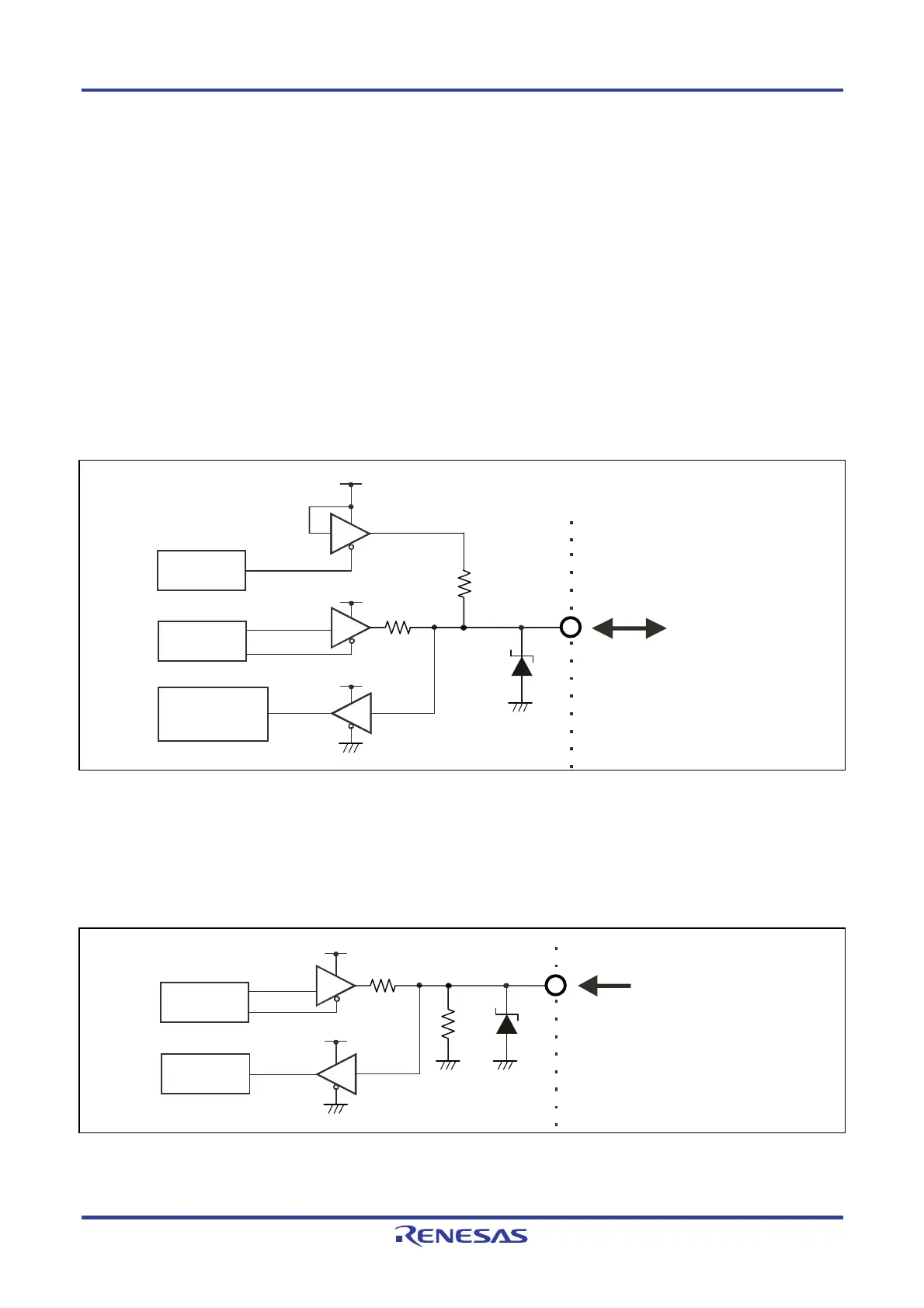
11.1 SO/TxD, RESET
¯¯¯¯¯¯
and SCK
When V
DD/VDD2 are supplied from the target system for target device programming, the FP5 internal voltage regulator is
protected so that user VDD/VDD2 will not affect the SO/TxD, RESET
¯¯¯¯¯¯
and SCK signal lines.
In either case, these signal lines output C-MOS level signals. When a 78K0R, 78K0S/Kx1+ microcontrollers or the
μ
PD78F9334 is used, the SO/TxD signal line functions as an open-drain output.
Figure 11-1. SO/TxD, RESET
¯¯¯¯¯¯
and SCK Pins
11.2 SI/RxD and H/S
The SI/RxD input signal voltages must not exceed the rated maximum voltage.
Figure 11-2. SI/RxD and H/S Pins
1 k
FP5
74LV125
74LV125
Signal
33
Target System
EMZ6.8 E
74LV125
FP5_VDD
FP5_VDD
FP5_VDD
Pull-up control
circuit
Signal output
circuit
Self-testing circuit
or signal input
circuit
FP5
33 Ω
EMZ6.8 E
Self-testing
circuit
Signal input
circuit
74LV125
74LV125
FP5_VDD
Signal
Target System
100 kΩ
FP5_V
DD
 Loading...