Doping profile
The doping profile of the device is derived from the C-V curve based on the definition of the
differential capacitance (measured by the 590 and 595) as the differential change in depletion region
charge produced by a differential change in gate voltage (Nicollian and Brews 380-389).
Depletion depth versus gate voltage (VGS)
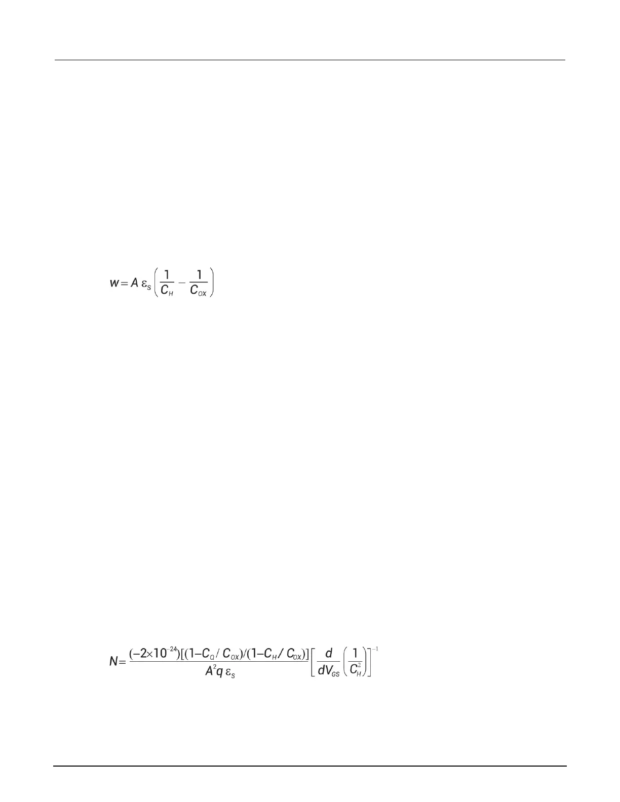
The Model 82 computes the depletion depth, w, from the high-frequency capacitance and oxide
capacitance at each measured value of V
GS
(Nicollian and Brews 386). In order to graph this function,
the program computes each w element of the calculated data array as shown below:
Where:
• w = depth (µm)
•
S
= permittivity of substrate material
• C
H
= high-frequency capacitance (pF)
• C
OX
= oxide capacitance (pF)
• A = gate area (cm
2
)
1/C^2 versus gate voltage
A 1/C
2
graph can yield important information about doping profile. N is related to the reciprocal of the
slope of the 1/C
2
versus V
GS
curve, and the V intercept point is equal to the flatband voltage caused
by surface charge and metal-semiconductor work function (Nicollian and Brews 385).
Doping concentration versus depth
The standard N versus w analysis discussed here does not compensate for the onset of accumulation,
and it is accurate only in depletion. This method becomes inaccurate when the depth is less than two
Debye lengths.
In order to correct for errors caused by interface traps, the error term (l-C
Q
/C
OX
)/1-C
H
/C
OX
) is included
in the calculations as follows:
 Loading...