5. Enter the label and wafer diameter in the Wafer Map Wizard window.
6. Click Next.
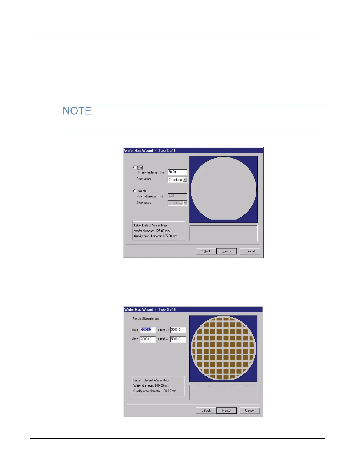
7. Select Flat or Notch based on the actual wafer.
8. Enter either the primary flat length or the notch diameter in millimeters.
9. Select the orientation of the flat or notch as applicable.
Bottom is toward the front of the prober.
Figure 252: Step 2: Wafer Map Wizard
10. Click Next.
11. Enter the correct die and street sizes.
Figure 253: Step 3: Wafer Map Wizard
 Loading...