List of Tables xi
List of Tables
Table 2-1. IMPRES Batteries ................................................................................................................. 2-1
Table 3-1. Battery Connector J3 ............................................................................................................ 3-5
Table 3-2. DC Supplies and Sources for Controller ............................................................................. 3-25
Table 3-3. MAKO’s LDO and Supplies................................................................................................. 3-25
Table 3-4. Pulse Switching Combination ............................................................................................. 3-27
Table 3-5. Controller Clock Distribution ............................................................................................... 3-29
Table 3-6. P1 Pin Assignment ............................................................................................................. 3-40
Table 3-7. GCAI Connector Pin Assignment........................................................................................ 3-41
Table 3-8. Secure Board KIT Numbers................................................................................................ 3-43
Table 3-9. Power and I/O Pins for NL5500 .......................................................................................... 3-45
Table 3-10. SPI Interface ....................................................................................................................... 3-46
Table 3-11. Register Address Map ........................................................................................................ 3-47
Table 3-12. Bluetooth Host Processor UART I/O................................................................................... 3-54
Table 3-13. SPI I/O ................................................................................................................................ 3-55
Table 3-14. USB I/O............................................................................................................................... 3-56
Table 3-15. GPIO I/O ............................................................................................................................. 3-57
Table 4-1. Recommended Service Tools ............................................................................................... 4-2
Table 4-2. Standard Operating Bias – DC Voltages............................................................................... 4-3
Table 4-3. Standard Operating Bias – Clock Sources............................................................................ 4-3
Table 4-4. Power-Up Self-Check Error Codes .......................................................................................4-4
Table 4-5. Power-Up Self-Check Diagnostic Actions............................................................................. 4-5
Table 5-1. Troubleshooting Charts......................................................................................................... 5-1
Table 6-1. List of Waveforms ................................................................................................................. 6-1
Table 6-2. Bluetooth Command to TX ................................................................................................. 6-38
Table 6-3. Bluetooth Command to RX ................................................................................................. 6-39
Table 6-4. Low Frequency Command to TX ........................................................................................ 6-39
Table 6-5. Low Frequency Command to RX........................................................................................ 6-39
Table 6-6. Bluetooth Test Points .......................................................................................................... 6-40
Table 7-1. List of Tables of Board and IC Signals .................................................................................. 7-1
Table 7-2. Mainboard to main flex connector interface Pin-Out............................................................. 7-2
Table 7-3. Main Flex connector to main board connector interface Pin-Out.......................................... 7-3
Table 7-4. Side Button Flex connector Pin-Out...................................................................................... 7-4
Table 7-5. Top Control Flex connector Pin-Out...................................................................................... 7-4
Table 7-6. NFC Flex connector interface Pin-Out..................................................................................7-5
Table 7-7. Overall GPIO pin functions ................................................................................................... 7-5
Table 7-8. Primary IC Reference Designator .......................................................................................7-13
Table 8-1. List of Transceiver Schematics and Board Overlays ............................................................ 8-1
Related Publications
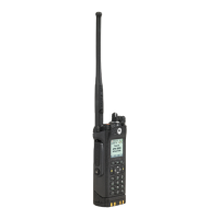
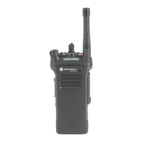
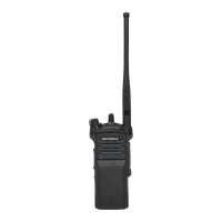
APX 3000 Digital Portable Radios Basic Service Manual ........................................................ 68012007044
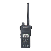
APX 3000 Digital Portable User Guide..................................................................................... 68012007043
 Loading...