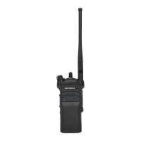
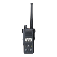
3-10 Theory of Operation: Main Board
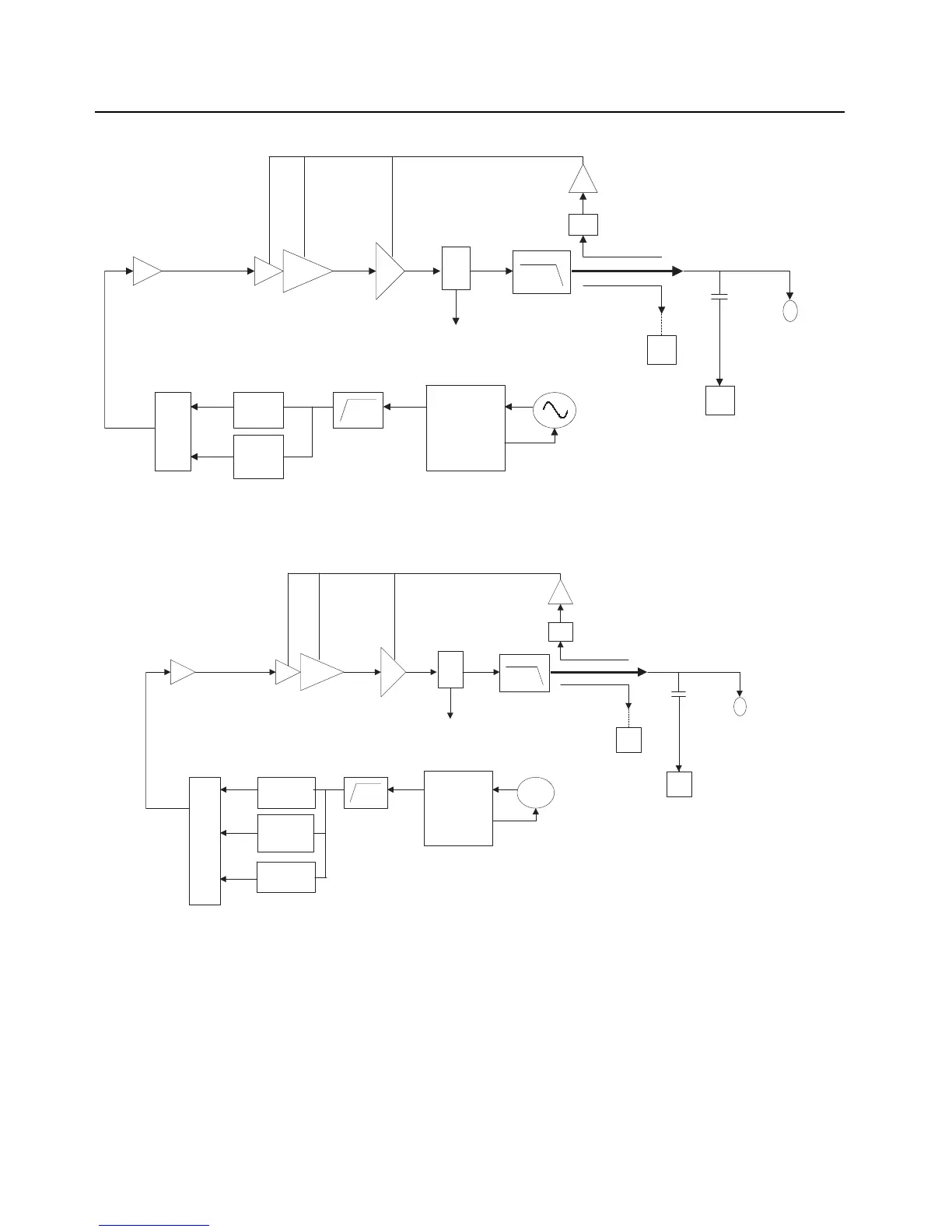
Figure 3-10. Transmitter Block Diagram (VHF)
Figure 3-11. Transmitter Block Diagram (700/800 MHz)
3.1.3.1 Driver Amplifier
The driver amplifier IC (UHF1/ UHF2 – U1602, VHF– U902 and 700/800 MHz– U1002) contains one
LDMOS FET amplifier stages and an internal resistor bias networks. Pin 16 is the RF input.
Modulated RF from the FGU, at a level of +3 dBm ±2 dB, is coupled through a blocking capacitor to
the gate of FET-1. An LC inter-stage matching network connects the first stage output VD1 to the
second stage input G2. The RF output from the drain of FET-2 is pin 6 (RFOUT1). Gain control is
provided by a voltage applied to pin 1 (VCNTRL). Typical output power is about +27 dBm (500 mW)
with VCNTRL at 5.5 V.
Trident IC
Synthesizer
Loop Filter
TX VCO
RX
VCO
RF Switch Matrix
TX Buffer Amp
TX Driver Amplifier
Transmitter Final
FET VHF
Harmonic
LP Filter
Ref. Oscillator
Antenna Connector
Directional
Coupler
Antenna
Switch
TO RX
GPS
Reverse Power
Detection
Log Amp Power Detector
Digital RF Attenuator
S
Trident IC
Synthesizer
Loop Filter
700 MHz
VCO
7/800 MHz
VCO
RF Switch Matrix
TX Buffer Amp
TX Driver Amplifier
Transmitter Final
FET 7/800 MHz
Harmonic
LP Filter
Ref. Oscillator
Antenna Connector
Directional
Coupler
Antenna
Switch
TO RX
GPS
Reverse Power
Detection
Log Amp Power Detector
Digital RF Attenuator
800 MHz
VCO
 Loading...