Home
Motorola
Two-Way Radio
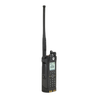
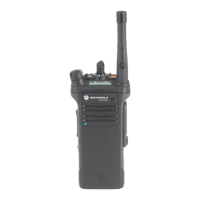
APX 3000
Motorola APX 3000 Detailed Service Manual
4
of 1
of 1 rating
474 pages
Give review
Manual
Specs
To Next Page
To Next Page
To Previous Page
To Previous Page
Loading...
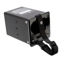
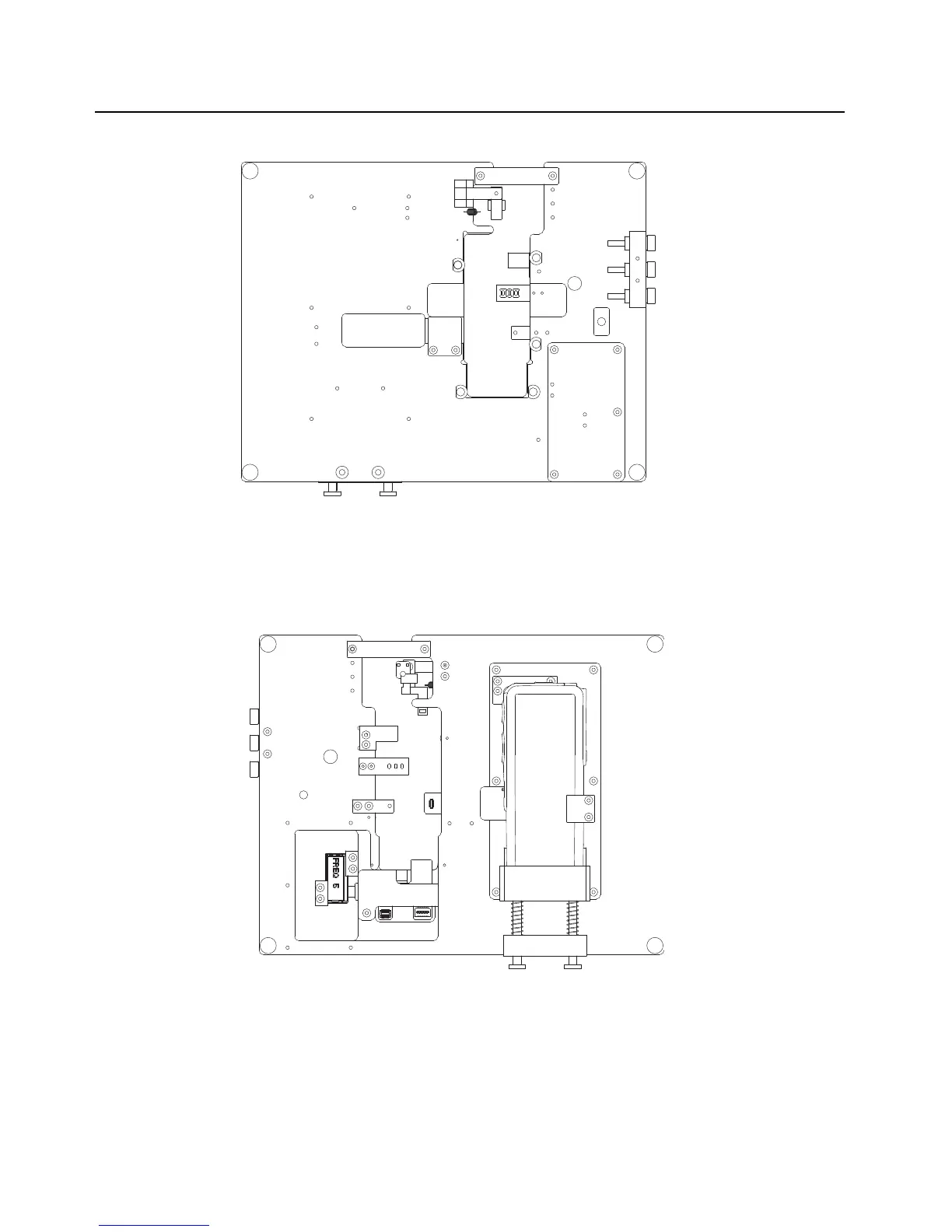
9-2
Debugging Fixture
:
Covert Board Debugging Fixture (Back)
9.2
Covert Board Debugging Fixture (Back)
Figure 9-2
. Covert Bo
ard Debugg
ing Fixture
(Back)
9.3
Covert Board Debugging Fixture
with Flexes, Housing and Display
(Front)
Figure 9-3. Covert Boar
d Debugging Fixtur
es with Flexe
s, Housing and Display (Fro
nt)
449
451
Table of Contents
Foreword
3
Manual Revisions
3
Product Safety and Rf Exposure Compliance
3
Computer Software Copyrights
3
Document Copyrights
3
Disclaimer
3
Trademarks
3
Document History
5
Table of Contents
7
List of Tables
11
Related Publications
11
List of Figures
13
Commercial Warranty
19
Limited Warranty
19
Motorola Communication Products
19
Chapter 1 Introduction
23
General
23
Notations Used in this Manual
24
Chapter 2 Radio Power
25
General
25
Table 2-1. IMPRES Batteries
25
DC Power Routing
26
Figure 2-1. DC Power Distribution
26
Chapter 3 Theory of Operation
27
Main Board
28
Figure 3-1. APX 3000 Overall Block Diagram
28
Figure 3-2. Transceiver (UHF1/ UHF2) Block Diagram (Power and Control Omitted)
29
Figure 3-3. Transceiver (VHF) Block Diagram (Power and Control Omitted)
30
Figure 3-4. Transceiver (700/800 Mhz) Block Diagram (Power and Control Omitted)
31
Table 3-1. Battery Connector J3
31
Figure 3-5. Receiver Block Diagram (UHF1)
32
Figure 3-6. Receiver Block Diagram (UHF2)
33
Figure 3-7. Receiver Block Diagram (VHF)
33
Figure 3-8. Receiver Block Diagram (700/800 Mhz)
33
Figure 3-9. Transmitter Block Diagram (UHF1/ UHF2)
35
Figure 3-10. Transmitter Block Diagram (VHF)
36
Figure 3-11. Transmitter Block Diagram (700/800 Mhz)
36
Directional Coupler
37
Harmonic Filter
37
Antenna Switch
38
Figure 3-12. Synthesizer Block Diagram (UHF1/ UHF2)
40
Figure 3-13. Synthesizer Block Diagram (VHF)
41
Figure 3-14. Synthesizer Block Diagram (700/800 Mhz)
41
Controller
47
Figure 3-15. Controller Interconnection Diagram
47
Figure 3-16. Controller Electrical Overview
49
Figure 3-17. Controller DC Block Diagram
50
Table 3-2. DC Supplies and Sources for Controller
51
Table 3-3. Mako's LDO and Supplies
51
Figure 3-18. V_SW_1.4 Switched Power Supply
52
Table 3-4. Pulse Switching Combination
53
Figure 3-19. 5V Switched Power Supply
53
Figure 3-20. Power-Up Timing Regulators
54
Table 3-5. Controller Clock Distribution
55
Figure 3-21. Controller Clock Architecture
55
Figure 3-22. Overview of OMAP Interconnection with Controller Peripherals
56
Figure 3-23. OMAP Memory Interface
57
Figure 3-24. RX / TX SSI Configuration
58
Figure 3-25. Audio SSI Configuration
59
Figure 3-26. SPI and I2C Configuration
60
Figure 3-27. CPLD Block Diagram
61
Figure 3-28. Audio TX Path Block Diagram
62
Figure 3-29. RX Audio Path Block Diagram
63
Figure 3-30. Control Top Block Diagram
64
User Interface
64
Figure 3-31. GCAI Signal Configuration
65
Side Controls
65
Table 3-6. P1 Pin Assignment
66
Figure 3-32. GCAI Connector
66
Table 3-7. GCAI Connector Pin Assignment
67
Figure 3-33. APX 3000 Encryption Architecture
68
Table 3-8. Secure Board KIT Numbers
69
Global Positioning System (GPS)
70
Table 3-9. Power and I/O Pins for NL5500
71
Figure 3-34. GPS Block Diagram
71
Accelerometer
72
Table 3-10. SPI Interface
72
Figure 3-35. Accelerometer Block Diagram
72
Table 3-11. Register Address Map
73
Bluetooth
74
Figure 3-36. Relation of Bluetooth & LF Antenna Assembly to Main Board
74
Figure 3-37. Bluetooth Connection Flowchart
75
Figure 3-38. Bluetooth/Controller Interface with Clock Sources
76
Figure 3-39. Bluetooth Functional Block Diagram
76
Figure 3-40. Bluetooth Low-Frequency Circuit Block Diagram
77
Figure 3-41. Bluetooth Low-Frequency Pairing Data Path
77
Figure 3-42. Detailed Low-Frequency Transmit/Receive Paths
78
Figure 3-43. Chip Power-Up/Power-Down Sequence (Exernal Input/Output Shown)
78
Figure 3-44. Current Distribution Tree for Bluetooth Circuitry
79
Table 3-12. Bluetooth Host Processor UART I/O
80
Table 3-13. SPI I/O
81
Figure 3-45. Bluetooth LF UART Connection Block Diagram
81
Table 3-14. USB I/O
82
Figure 3-46. Bluetooth USB Interface to Main Board
82
Table 3-15. GPIO I/O
83
Chapter 4 Troubleshooting Procedures
85
Handling Precautions
85
Recommended Service Tools
86
Table 4-1. Recommended Service Tools
86
Standard Bias Table
87
Table 4-2. Standard Operating Bias - DC Voltages
87
Table 4-3. Standard Operating Bias - Clock Sources
87
Power-Up Self-Check Errors
88
Table 4-4. Power-Up Self-Check Error Codes
88
Power-Up Self-Check Diagnostics and Repair (Not for Field Use)
89
Table 4-5. Power-Up Self-Check Diagnostic Actions
89
Chapter 5 Troubleshooting Charts
91
List of Troubleshooting Charts
91
Table 5-1. Troubleshooting Charts
91
Main Troubleshooting Flowchart
93
Power-Up Failure
94
DC Supply Failure
105
Side Button Error
112
RX Audio Error
113
TX Audio Error
114
Keyload Failure
115
Secure Hardware Failure
116
RX RF Failure
117
5.11 FGU Failure
127
VCO Failure
129
5.13 GPS Failure
133
5.14 Bluetooth Failure - Pairing Issue
134
PA Failure
141
Chapter 6 Troubleshooting Waveforms
145
List of Waveforms
145
Table 6-1. List of Waveforms
145
Clocks
146
Figure 6-1. 32 Khz Clock Waveform
146
Figure 6-2. 4 Mhz Clock Waveform
147
Figure 6-3. 12 Mhz Clock Waveform
148
Figure 6-4. 16.8 Mhz Clock Waveform
149
Figure 6-5. 24 Mhz Clock Waveform
150
Audio SSI
151
Figure 6-6. Audio SSI - Red Tx Waveform
151
Figure 6-7. Audio SSI - Red Rx Waveform
152
Figure 6-8. Audio SSI - Sync. Waveform
153
Figure 6-9. Audio SSI - BCLK. Waveform
154
Rx Ssi
155
Figure 6-10. RX SSI - CLK. Waveform
155
Figure 6-11. RX SSI - da Waveform
156
Figure 6-12. RX SSI - Fsync. Waveform
157
Tx Ssi
158
Figure 6-13. TX SSI - TX CLK. Waveform
158
Figure 6-14. TX SSI - da Waveform
159
Figure 6-15. TX SSI - Fsync. Waveform
160
Spi
161
Figure 6-16. SPI - CLK Waveform
161
Figure 6-17. CS Waveform
162
I2C Bus
163
Figure 6-18. I2C Bus - SCA Waveform
163
Figure 6-19. I2C Bus - SCA 5V Waveform
164
Figure 6-20. I2C Bus - SDA Waveform
165
One Wire
166
Figure 6-21. 1-Wire Waveform
166
Gcai
167
Figure 6-22. GCAI - GPIO0 Waveform
167
Figure 6-23. GCAI - GPIO4 Waveform
168
6.10 Usb
169
Figure 6-24. USB - D- Waveform
169
Figure 6-25. USB - D+ Waveform
170
6.11 Sdram
171
Figure 6-26. SDRAM - CLK Waveform
171
Figure 6-27. SDRAM - CLKX Waveform
172
6.12 Flash Control
173
Figure 6-28. FLASH CONTROL - ADV Waveform
173
Figure 6-29. FLASH CONTROL - CS3 Waveform
174
Figure 6-30. FLASH CONTROL - OE Waveform
175
Figure 6-31. FLASH CONTROL - RDY Waveform
176
Figure 6-32. FLASH CONTROL - WE Waveform
177
6.13 Receive Baseband Signals
178
Figure 6-33. Received Baseband Waveforms
178
6.14 Gps
179
Figure 6-34. GPS TCXO Waveforms
179
Figure 6-35. GPS RTC Waveforms
180
Figure 6-36. GPS UART DATA Waveforms
181
6.15 Bluetooth Troubleshooting Waveforms
182
Table 6-2. Bluetooth Command to TX
182
Table 6-3. Bluetooth Command to RX
183
Table 6-4. Low Frequency Command to TX
183
Table 6-5. Low Frequency Command to RX
183
Table 6-6. Bluetooth Test Points
184
Figure 6-37. Summary of Bluetooth Power up Sequence
184
Figure 6-38. Startup Waveforms - Vmax of TP16
185
Figure 6-39. Startup - Timing Difference of TP9 to TP16
186
Figure 6-40. Startup - Timing Difference of TP5 to TP16 and Voltage Statistics
187
Figure 6-41. Startup - Timing Difference of TP4 to TP16 and Time Statistics
188
Figure 6-42. Startup - Timing Difference of TP4 to TP5 and Time Statistics
189
Figure 6-43. Startup - Vmax of TP5 and Time Statistics
190
Figure 6-44. Startup - Vmax of TP4 and Time Statistics
191
Figure 6-45. Startup - Vmax of TP5 and Voltage Statistics
192
Figure 6-46. Startup - Vmax of TP9 and Voltage Statistics
193
Figure 6-47. Startup - Vmax of TP10 and Time Statistics
194
Figure 6-48. Startup - Vmax of TP16 and Voltage Statistics
195
Figure 6-49. Startup - Vmax of TP13 and Voltage Statistics
196
Figure 6-50. Startup - Vmax of TP11 and Voltage Statistics
197
Figure 6-51. Startup - Timing Difference of TP13 to TP16 and Time Statistics
198
Figure 6-52. Startup - Timing Difference of TP10 to TP13 and Time Statistics
199
Figure 6-53. Startup - Timing Difference of TP11 to TP13 and Time Statistics
200
Figure 6-54. Bluetooth CW on Spectrum Analyzer
201
6.16 Bluetooth Steady-State
202
Figure 6-55. USB D+ Vmax and Packet Timing with Statistics
202
Figure 6-56. USB D- Vmax and Packet Timing with Statistics
203
Figure 6-57. V_SW_3.6 Voltage Statistics
204
Figure 6-58. 32 Khz Clock Vmax with Statistics
205
Figure 6-59. LF Coil When TX and RX
206
6.17 LF CW on Spectrum Analyzer
207
Figure 6-60. LF CW on Spectrum Analyzer
207
Chapter 7 Troubleshooting Tables
209
List of Board and IC Signals
209
Table 7-2. Mainboard to Main Flex Connector Interface Pin-Out
210
Table 7-3. Main Flex Connector to Main Board Connector Interface Pin-Out
211
Table 7-4. Side Button Flex Connector Pin-Out
212
Table 7-5. Top Control Flex Connector Pin-Out
212
Table 7-6. NFC Flex Connector Interface Pin-Out
213
Table 7-7. Overall GPIO Pin Functions
213
Table 7-8. Primary IC Reference Designator
221
Chapter 8 Schematics, Boards Overlays, and Parts Lists
223
List of Transceiver Schematics and Board Overlays
223
Table 8-1. List of Transceiver Schematics and Board Overlays
223
Figure 8-114.Connectors
223
Main Board Block: UHF1 (84012513001_A)
225
Figure 8-1. Main Board Block
225
Figure 8-2. Transceiver (RF) Board Overall Schematic Blocks
226
Figure 8-3. Antenna Switch Circuit
227
Figure 8-4. Transmitter HF Circuit
228
Figure 8-5. Power Amplifier Circuit
229
Figure 8-6. Automatic Level Control Circuit
230
Figure 8-7. Receiver Front End Circuit
231
Figure 8-8. Receiver Back End Mixer
232
Figure 8-9. Receiver Back End
233
Figure 8-10. Receiver VCO Circuit
234
Figure 8-11. Transmitter VCO Circuit
235
Figure 8-14. DC Circuit
238
Figure 8-15. Controller Overall Schematic Blocks
239
Figure 8-18. Top Control and JTAG Circuit
242
Figure 8-19. Lighting Control Circuit
243
Figure 8-20. GCAI and Side Control
244
Figure 8-21. Debugging and Display Connector
245
Figure 8-22. Connectors
246
Figure 8-23. CPLD Circuit
247
Figure 8-24. OMAP User Interface Circuit
248
Figure 8-25. Memory Interface
249
Figure 8-26. Audio Circuit
250
Figure 8-27. MAKO/DC Distribution Circuit
251
Figure 8-28. Serial Interface Circuit
252
Figure 8-29. Secure Circuit
253
Figure 8-30. Transceiver (RF) Board Layout - Top Side
254
Figure 8-31. Transceiver (RF) Board Layout - Bottom Side
255
Main Board Block: 700-800 Mhz (84012501002)
283
Figure 8-32. Main Board Block
283
Figure 8-33. Transceiver (RF) Board Overall Schematic
284
Figure 8-34. Receiver Back End
285
Figure 8-37. Automatic Level Control Circuit
288
Figure 8-38. VCO Circuit
289
Figure 8-39. Receiver Front End Circuit
290
Figure 8-40. Receiver Back End Mixer
291
Figure 8-41. Power Amplifier Circuit
292
Figure 8-42. DC Circuit
293
Figure 8-43. Antenna Switch Circuit
294
Figure 8-44. Transmitter HF Circuit
295
Figure 8-45. Controller Overall Schematic Blocks
296
Figure 8-48. Top Control and JTAG Circuit
299
Figure 8-49. Lighting Control Circuit
300
Figure 8-50. GCAI and Side Control
301
Figure 8-51. Debugging and Display Connector
302
Figure 8-52. Connectors
303
Figure 8-53. CPLD Circuit
304
Figure 8-54. OMAP User Interface Circuit
305
Figure 8-55. Memory Interface
306
Figure 8-56. Audio Circuit
307
Figure 8-57. MAKO/DC Distribution Circuit
308
Figure 8-58. Serial Interface Circuit
309
Figure 8-59. Secure Circuit
310
Figure 8-60. Transceiver (RF) Board Layout - Top Side
311
Figure 8-61. Transceiver (RF) Board Layout - Bottom Side
312
Main Board Block: VHF (84012512001_A)
339
Figure 8-62. Main Board Block
339
Figure 8-63. Transceiver (RF) Board Overall Schematic
340
Figure 8-64. ANTSWI Circuit
341
Figure 8-65. Transmitter HF Circuit
342
Figure 8-66. Power Amplifier Circuit
343
Figure 8-67. Automatic Level Control Circuit
344
Figure 8-68. Receiver Front End Circuit
345
Figure 8-69. Receiver Back End Mixer
346
Figure 8-70. Receiver Back End
347
Figure 8-71. Receiver VCO Circuit
348
Figure 8-72. Transmitter VCO Circuit
349
Figure 8-75. DC Circuit
352
Figure 8-76. Controller Overall Schematic Blocks
353
Figure 8-79. Top Control and JTAG Circuit
356
Figure 8-80. Lighting Control Circuit
357
Figure 8-81. GCAI and Side Control
358
Figure 8-82. Debugging and Display Connector
359
Figure 8-83. Connectors
360
Figure 8-84. CPLD Circuit
361
Figure 8-85. OMAP User Interface Circuit
362
Figure 8-86. Memory Interface
363
Figure 8-87. Audio Circuit
364
Figure 8-88. MAKO/DC Distribution Circuit
365
Figure 8-89. Serial Interface Circuit
366
Figure 8-90. Secure Circuit
367
Figure 8-91. Transceiver (RF) Board Layout - Top Side
368
Figure 8-92. Transceiver (RF) Board Layout - Bottom Side
369
Main Board Block: UHF2 (84012616001)
391
Figure 8-93. Main Board Block
391
Figure 8-94. Transceiver (RF) Board Overall Schematic
392
Figure 8-95. ANTSWI Circuit
393
Figure 8-96. Transmitter HF Circuit
394
Figure 8-97. Power Amplifier Circuit
395
Figure 8-98. Automatic Level Control Circuit
396
Figure 8-99. Receiver Front End Circuit
397
Figure 8-100.Receiver Back End Mixer
398
Figure 8-101.Receiver Back End
399
Figure 8-102.Receiver VCO Circuit
400
Figure 8-103.Transmitter VCO Circuit
401
Figure 8-106.DC Circuit
404
Figure 8-107.Controller Overall Schematic Blocks
405
Figure 8-110.Top Control and JTAG Circuit
408
Figure 8-111.Lighting Control Circuit
409
Figure 8-112.GCAI and Side Control
410
Figure 8-113.Debugging and Display Connector
411
Figure 8-115.CPLD Circuit
413
Figure 8-116.OMAP User Interface Circuit
414
Figure 8-117.Memory Interface
415
Figure 8-118.Audio Circuit
416
Figure 8-119.MAKO/DC Distribution Circuit
417
Figure 8-120.Serial Interface Circuit
418
Figure 8-121.Secure Circuit
419
Figure 8-122.Transceiver (RF) Board Layout - Top Side
420
Figure 8-123.Transceiver (RF) Board Layout - Bottom Side
421
Chapter 9 Debugging Fixture
449
Covert Board Debugging Fixture (Front)
449
Covert Board Debugging Fixture (Back)
450
Covert Board Debugging Fixture with Flexes, Housing and Display (Front)
450
Figure 9-3. Covert Board Debugging Fixtures with Flexes, Housing and Display (Front)
450
Covert Board Debugging Fixture with Flexes, Housing and Display (Back)
451
Debugging Fixture Set up
451
Figure 9-4. Covert Board Debugging Fixture with Flexes, Housing and Display (Back)
451
Figure 9-5. Remove the Housing Clamp
451
Figure 9-6. Remove the Display Clamp
452
Figure 9-7. Remove Transparent Cover (1)
452
Figure 9-8. Remove Transparent Cover (2)
453
Figure 9-9. Assemble NFC Flex
453
Board Assembly on Debugging Fixture
454
Figure 9-10. Board Assembly
454
Powering up Covert Board
455
Figure 9-11. Power up Covert Board
455
Appendix A Replacement Parts Ordering
457
Basic Ordering Information
457
Transceiver Board, Controller Board and Expander Board Ordering Information
457
Motorola Online
457
Mail Orders
457
Telephone Orders
457
Fax Orders
458
Parts Identification
458
Product Customer Service
458
A.6 Fax Orders
458
Glossary
459
Index
469
Other manuals for Motorola APX 3000
User Guide
104 pages
Basic Service Manual
144 pages
Quick Reference Guide
44 pages
Quick Reference Card
92 pages
4
Based on 1 rating
Ask a question
Give review
Questions and Answers:
Need help?
Do you have a question about the Motorola APX 3000 and is the answer not in the manual?
Ask a question
Motorola APX 3000 Specifications
General
Brand
Motorola
Model
APX 3000
Category
Two-Way Radio
Language
English
Related product manuals
Motorola APX 3
48 pages
Motorola APX 8000 3
202 pages
Motorola APX 8500
273 pages
Motorola APX 7500
70 pages
Motorola APX 6000
200 pages
Motorola APX 4500
201 pages
Motorola APX 6500
52 pages
Motorola APX 8000
161 pages
Motorola APX 1000
166 pages
Motorola APX NEXT
119 pages
Motorola ASTRO APX
168 pages
Motorola APX Mobile
146 pages
 Loading...