3-52 Theory of Operation: Bluetooth
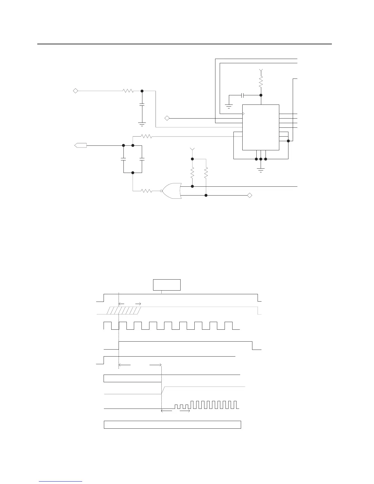
Figure 3-42. Detailed Low-Frequency Transmit/Receive Paths
3.5.1 Bluetooth Power
Our Bluetooth IC operates from a 3.6V (U6504, VBAT) switching regulator located on the Main board
to supply the Bluetooth IC core and a 1.85V (U6508, VDDS) supply for the I/O. It has a shutdown
(U2415 pin L3) that must be high for operation to work. The power-up/down sequence required for
operation is shown in Figure 3-43.
Figure 3-43. Chip Power-Up/Power-Down Sequence (Exernal Input/Output Shown)
32KHZ_3.3V
R2457
15K
C2475
1000PF
R2474
270K
NFC_ANTENNA
OUT
C2457
18PF
U2412
NL17SZ02
R2475M3
150
USART1_TX
R2477
100K
7
16
15
R2419
100
G1
R2476
100K
TC1_OCA
4
1
2
TX path
GPS_BT_3.3V
12
9
14
6
8
1
2
10
SCL
DAT
SDO
XOUT
WAKE
NC1
NC2
NC3
VCC
CS
SDI
XIN
LFN
LF1P
VSS
GND
CTGND
C2465
1UF
GPS_BT_3.3V
U2403M3
AS3930A
51009735001
11
13
5
4
3
RX path
NFC_CS_INV
C2454
220PF
1%
APX 3000
Partial Current Tree
7.5V Batt
VDDS
VBAT
VDD1P8
RTC
Startup
CLK_REQ_POL
TCXO_CLK_REQ
VDD_TCXO
Hi Z - PD
Max 36.5 ms
5 ms
Analog PORz (~135 RTC cycles) +
Efuse shifting (~1000 RTC cycles)
Max time from clock request/
voltage to TCXO_CLK availability
Hi Z - PD
TCXO_CLK
REF_CLK_REQ
(OR of
nshutdown
pins)
<2.5ms
or
 Loading...