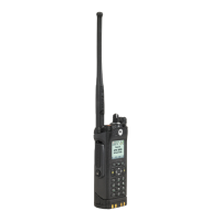
3-6 Theory of Operation: Main Board
3.1.1.2 Power Conditioning Components
DC power-conditioning components include zener diodes, capacitors, ferrite beads, a power
inductor, and the fuse. Diodes VR200 and VR101 provide over-voltage protection. Ferrite beads
(designated E, etc.) and capacitors suppress electromagnetic interference from the main board.
The power-line filter consisting of L200, C202, and C203 suppresses digital noise from the controller
board switching power supplies that could degrade the transmitter spectral purity.
Ground clips M103, M104 and M105 make contact between the main board ground and the radio
chassis. The chassis connection is a necessary electrical reference point to complete the antenna
circuit path. Shields SH1 through SH17 appear on the schematic to show their connection to ground.
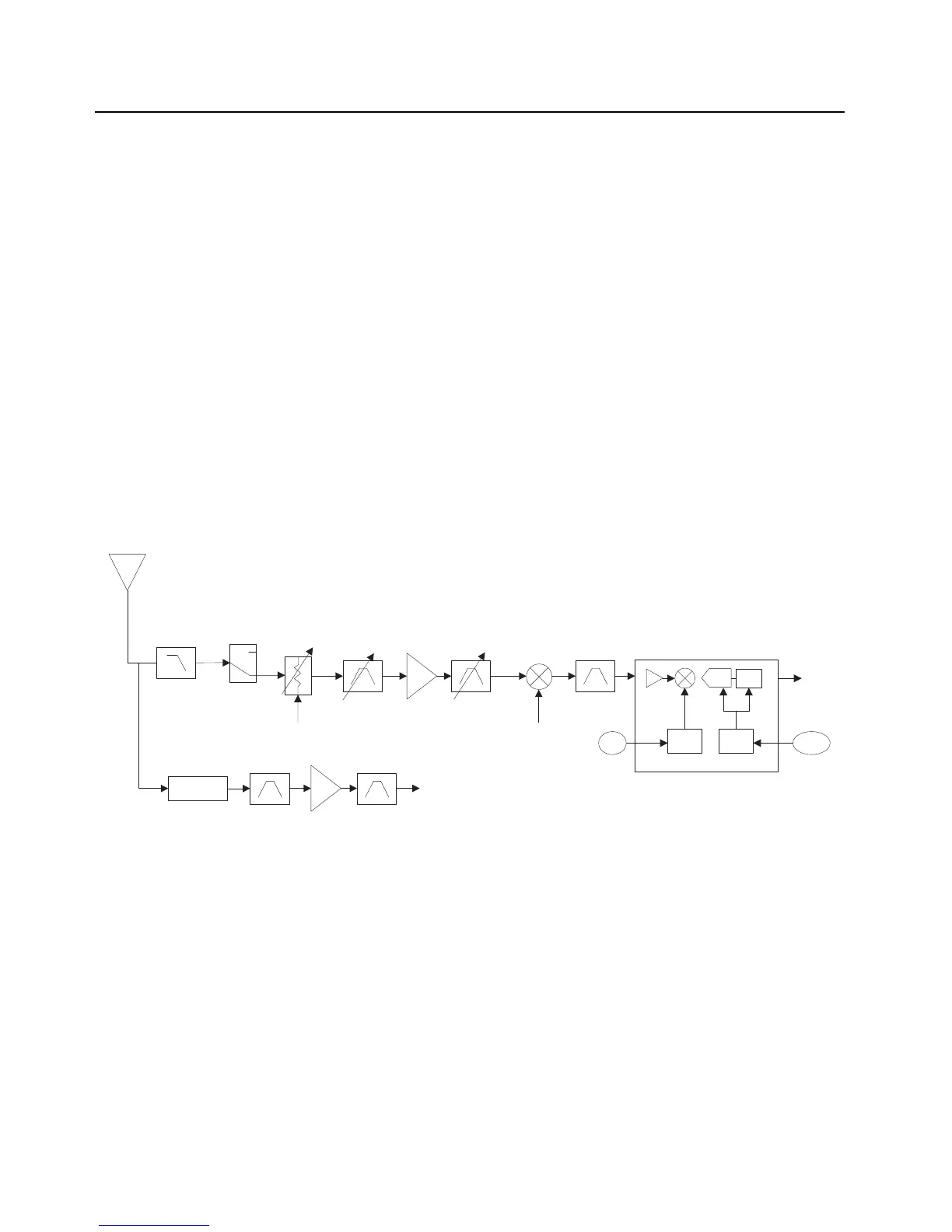
3.1.2 Receiver
The RF signal is received at the antenna and is routed through the Harmonic Filter, followed by the
Antenna Switch and the 15dB Step Attenuator IC. The latter contains a switchable attenuator that is
enabled at predetermined RF power thresholds present at the antenna port. The output of the
attenuator leads to the receiver front end section.
• UHF1/ UHF2 band (See Figure 3-5./ See Figure 3-6.)
• VHF band (See Figure 3-7.)
• 700/800 MHz band (See Figure 3-8.)
Figure 3-5. Receiver Block Diagram (UHF1)
Antenna
Switch
15 dB Step
Attenuator
UHF UHF
IF Filter
DIG_CTRL_ATTH Rx LO
To GPS
Diplexer
SSI
18Mhz
CLK
Abacus III
ABACUS III
Dec.
Filter
ΣΔ ADC
2nd
LO
LO CLK
Harmonic
Filter
 Loading...