December 6, 2004 68P81083C20-D
7-10 Controller Section Theory of Operation: Interfacing
Serial Peripheral Interface (SPI)
(Refer to Controller schematic page 10-23 for reference)
The µP communicates to many of the ICs through its SPI port. This port consists of SPI TX DATA
(U0103-66), SPI RX DATA (U0103-65), CLK (U0103-67) and chip select lines going to the various
ICs, connected on the SPI PORT (BUS). This BUS is a synchronous bus, in that the timing clock
signal CLK is sent while SPI data (SPI TX DATA or SPI RX DATA) is sent. Therefore, whenever there
is activity on either SPI TX DATA or SPI RX DATA there should be a uniform signal on CLK. The SPI
TX DATA is used to send serial from a µP to a device, and SPI RX DATA is used to send data from a
device to a µP.
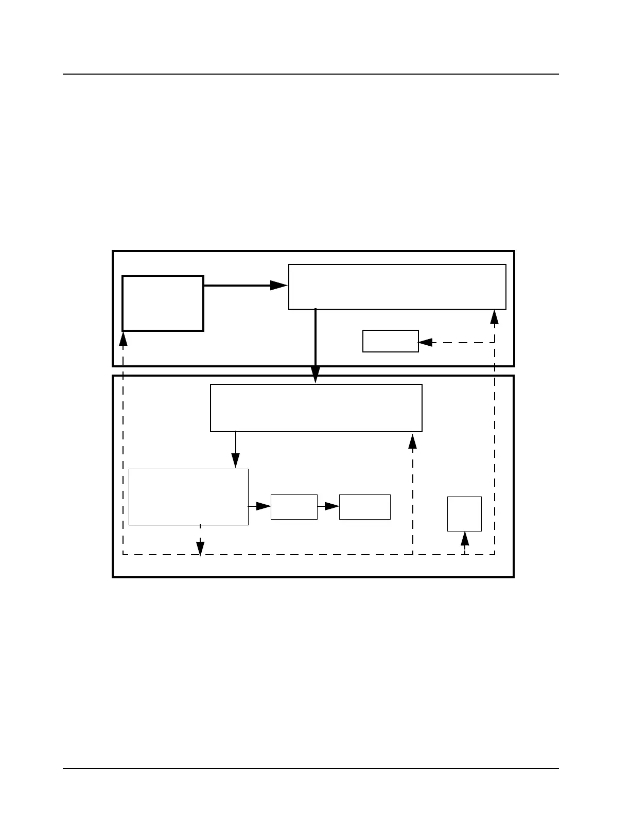
Figure 7-1. Clock Distribution Block Diagram
On the controller there are 2 ICs on the SPI BUS, ASFIC (U0200-F2) and D/A (U0551-6). In the UHF
and VHF RF sections there are 3 ICs on the SPI BUS, ZIF (U3201-21), Pendulum (Reference
Oscillator U5800-23) and FRAC/N (U5801-4). For the 800 and 900 MHz radios the 3 ICs on the SPI
BUS are: ZIF (U6201), Pendulum (Reference Oscillator U6704) and FRAC/N (U6702). The SPI TX
DATA and CLK lines going to the RF section are filtered by R0403 and R0404 to minimize noise.
There are 2 chip select lines going to each of the 2 Option boards (J0401-21 and J0401-23 /and
J0408-21 and J0408-23).
PENDULUM
QUARTZ
CRYSTAL
16.8 MHZ
FRACTIONAL DIVISION SYNTHESIZER
ELECTRONIC CLOCK GENERATION
2.1 MHz
ZERO I.F.
SPI-CLOCK
SPI-CLOCK
AUDIO SIGNALLING FILTER IC
ELECTRONIC CLOCK GENERATION,
PROGRAMMABLE RANGE:
1200 Hz to 32.769 MHz (1200 Hz STEPS)
68HC11K4 uP
D/A
MC68HC11F1 MICRO
CONTROLLER
ELECTRONIC GENERATION
OF E AND SPI CLOCKS
F REF OUT
E-CLOCK
SPI-CLOCK
TRANSCEIVER
CONTROLLER
SLIC IVa OR
SLIC V
(not placed in
this application)
uP-CLOCK
 Loading...