RL78/F13, F14 CHAPTER 25 POWER-ON-RESET CIRCUIT
R01UH0368EJ0210 Rev.2.10 1556
Dec 10, 2015
25.2 Configuration of Power-on-reset Circuit
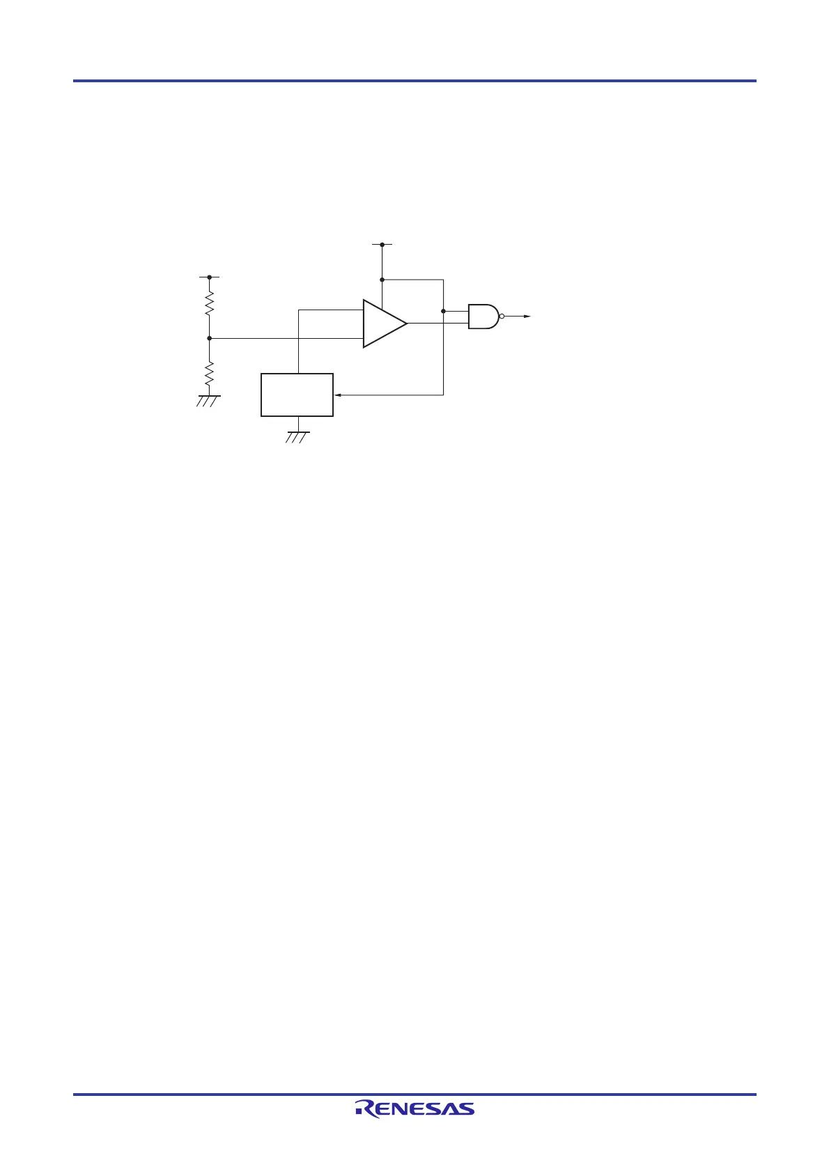
The block diagram of the power-on-reset circuit is shown in Figure 25-1.
Figure 25-1. Block Diagram of Power-on-reset Circuit
25.3 Operation of Power-on-reset Circuit
An internal reset signal is generated on power application. When the supply voltage (V
DD) exceeds the detection
voltage (V
POR = 1.56 V (typ.)
Note
), the reset status is released.
The supply voltage (V
DD) and detection voltage (VPDR = 1.55 V (typ.)
Note
) are compared. When VDD < VPDR, the internal
reset signal is generated.
Note When the user option byte function is used to enable the voltage detector by default, release from the reset state
does not proceed until the value set in the option byte function is exceeded.
The timing of generation of the internal reset signal by the power-on-reset circuit and voltage detector is shown below.
−
+
Reference
voltage
source
Internal reset signal
VDD
VDD
 Loading...


