RL78/F13, F14 CHAPTER 34 ELECTRICAL SPECIFICATIONS (GRADE L)
R01UH0368EJ0210 Rev.2.10 1686
Dec 10, 2015
34.3 DC Characteristics
34.3.1 Pin Characteristics
For the relationship between the port pins shown in the following tables and the products, refer to CHAPTER 4 PORT
FUNCTIONS.
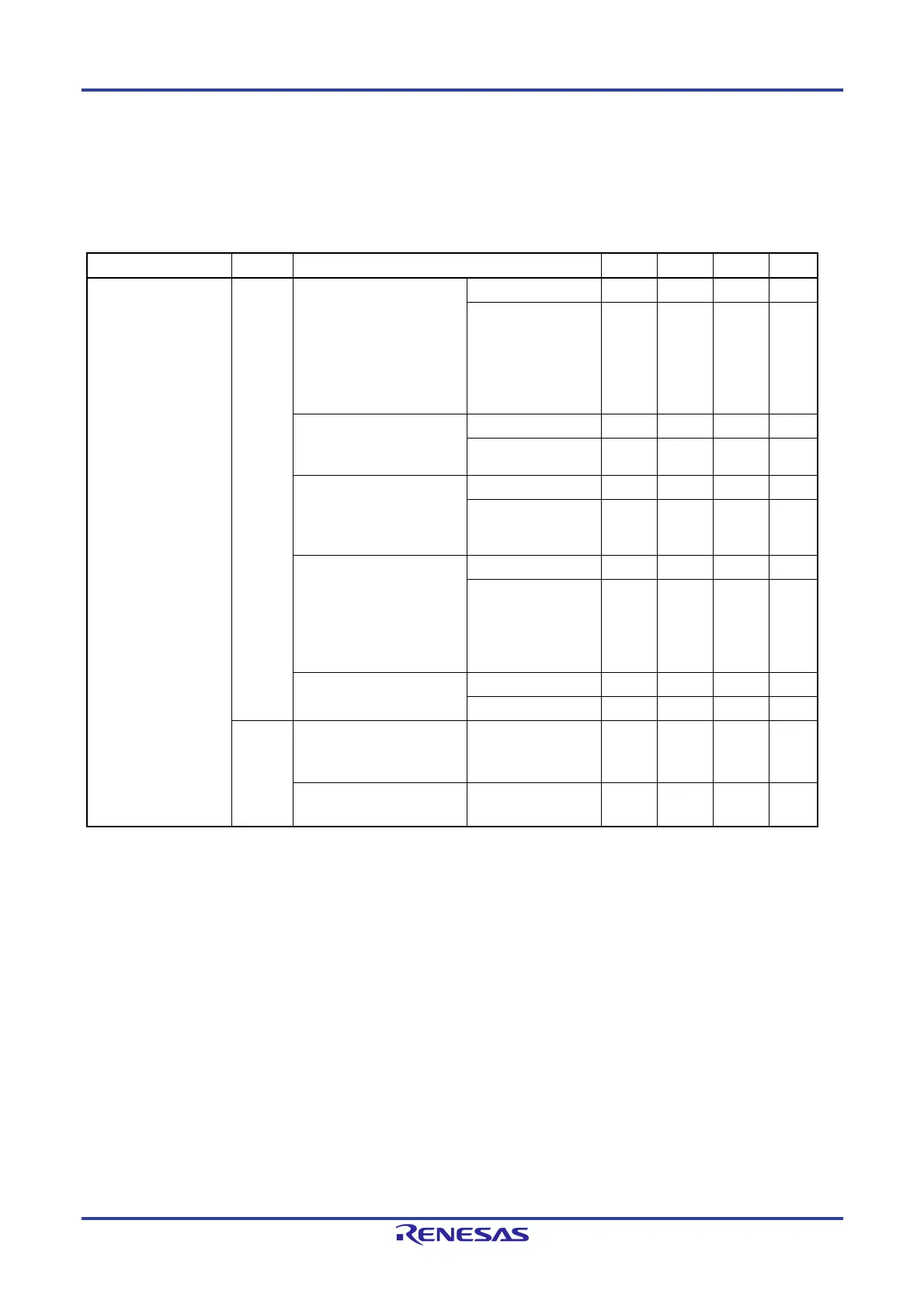
(T
A = -40 to +105C, 2.7 V EVDD0 = EVDD1 = VDD 5.5 V, VSS = EVSS0 = EVSS1 = 0 V) (1/4)
Items Symbol Conditions MIN. TYP. MAX. Unit
Output current, high
Note
1
I
OH1
Per pin for P00 to P03, P10
to P17, P30 to P32, P40 to
P47, P50 to P57, P60 to
P67, P70 to P77, P92 to
P97
Note 3
, P106, P107, P120,
P125 to P127, P130, P140,
P150 to 157
4.0 V EV
DD0 5.5 V
-5.0 mA
2.7 V EVDD0 < 4.0 V
-3.0 mA
Per pin for P10, P12, P14,
P30,P120,P140
(special slew rate)
4.0 V EV
DD0 5.5 V
-0.6 mA
2.7 V EVDD0 < 4.0 V
-0.2 mA
Total of P01, P02, P40 to
P47, P92 to P97
Note 3
, P120,
P125 to P127, P150 to P153
(for duty factors 70%
Note 2
)
4.0 V EV
DD0 5.5 V
-20.0 mA
2.7 V EVDD0 < 4.0 V
-10.0 mA
Total of P00, P03, P10 to
P17, P30 to P32, P50 to
P57, P60 to P67, P70 to
P77, P106, P107, P130,
P140, P154 to P157
(for duty factors 70%
Note 2
)
4.0 V EV
DD0 5.5 V
-30.0 mA
2.7 V EVDD0 < 4.0 V
-19.0 mA
Total of all pins
(for duty factors 70%
Note 2
)
4.0 V EV
DD0 5.5 V
-50.0 mA
2.7 V EVDD0 < 4.0 V
-29.0 mA
IOH2
Per pin for P33, P34, P80 to
P87, P90 to P97
Note 3
, P100
to P105
2.7 V V
DD 5.5 V -0.1 mA
Total of all pins
(for duty factors 70%
Note 2
)
2.7 V V
DD 5.5 V -2.0 mA
Notes 1. Value of current at which the device operation is guaranteed even if the current flows from pins EVDD0, EVDD1
and V
DD to an output pin.
2.
These output current values are obtained under the condition that the duty factor is no greater than 70%.
The output current values when the duty factor is changed to a value greater than 70% can be calculated
from the following expression (when the duty factor is changed to n%).
Total output current of pins (I
OH 0.7)/(n 0.01)
<Example> Where n = 80% and IOH = -10.0 mA
Total output current of pins = (-10.0 0.7)/(80 0.01) ≈ -8.7 mA
However, the current that is allowed to flow into one pin does not vary depending on the duty factor. A
current higher than the absolute maximum rating must not flow into one pin.
3. For pin I/O buffer power supplies, refer to Table 4-1 Pin I/O Buffer Power Supplies.
Caution P10 to P17, P60 to P63, P70 to P72, and P120 do not output high level in N-ch open-drain mode.
P10 to P12 and P70 to P72 of the Group A products do not support N-ch open-drain mode.
Remark Unless specified otherwise, the characteristics of alternate-function pins are the same as those of the port pins.
<R>
 Loading...


