RL78/F13, F14 CHAPTER 6 TIMER ARRAY UNIT
R01UH0368EJ0210 Rev.2.10 499
Dec 10, 2015
6.7.3 Operation as frequency divider
The timer array unit can be used as a frequency divider that divides a clock input to the TImn pin and outputs the result
from the TOmn pin.
Set the TImn and TOmn pins so that they are different from each other by the peripheral I/O redirection registers 0, 1, 2,
and 3 (PIOR0, PIOR1, PIOPR2, and PIOR3).
The divided clock frequency output from TOmn can be calculated by the following expression.
When rising edge/falling edge is selected:
Divided clock frequency = Input clock frequency/{(Set value of TDR00 + 1) 2}
When both edges are selected:
Divided clock frequency Input clock frequency/(Set value of TDR00 + 1)
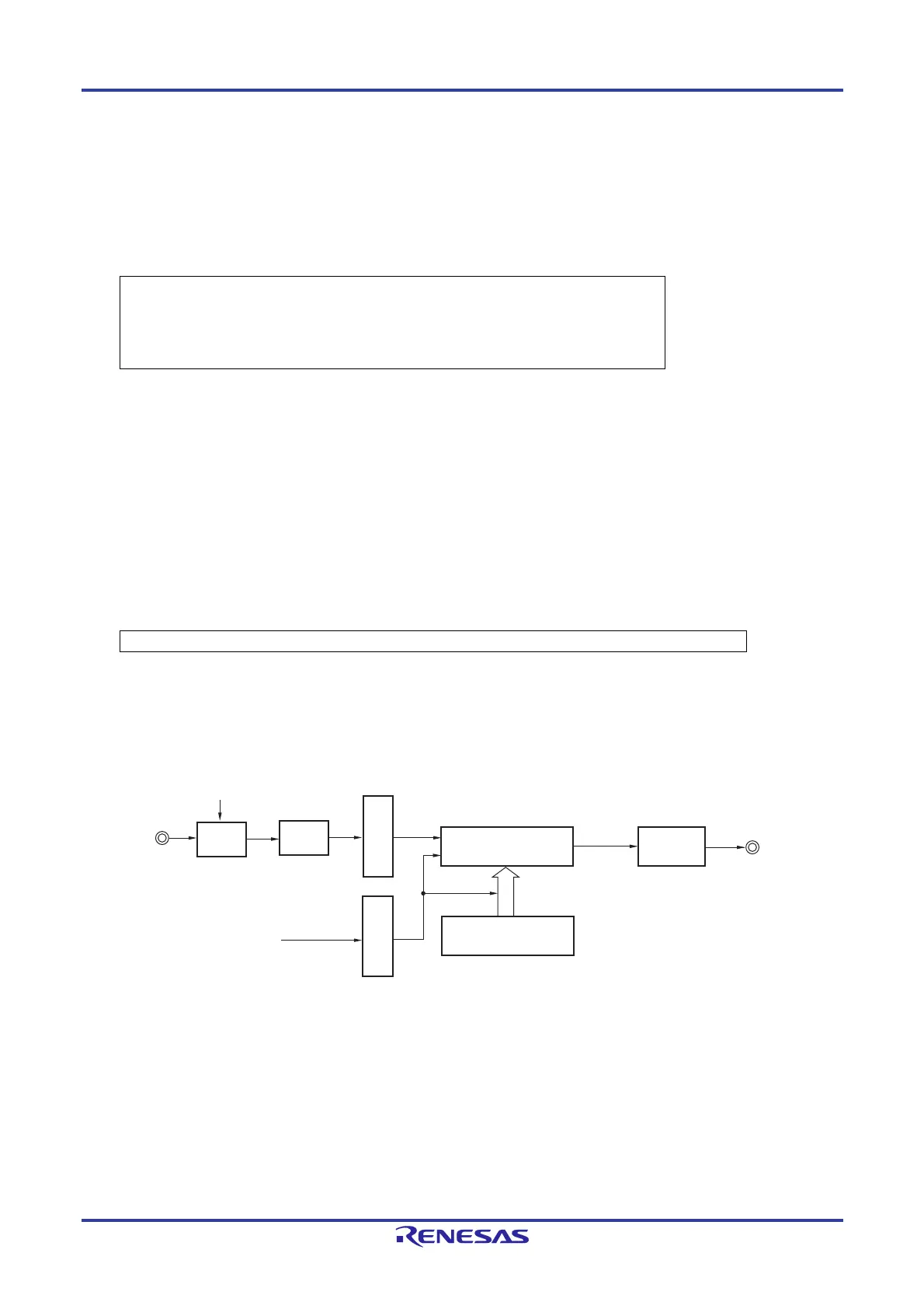
Timer count register m (TCRm) operates as a down counter in the interval timer mode.
After the channel start trigger bit (TS00) of timer channel start register 0 (TS0) is set to 1, the TCR00 register loads the
value of timer data register 00 (TDR00) when the TI00 valid edge is detected.
If the MNmn0 bit of timer mode register 00 (TMR00) is 0 at this time, INTTM00 is not output and TO00 is not toggled. If
the MNmn0 bit of timer mode register 00 (TMR00) is 1, INTTM00 is output and TO00 is toggled.
After that, the TCR00 register counts down at the valid edge of the TI00 pin. When TCR00 = 0000H, it toggles TO00. At
the same time, the TCR00 register loads the value of the TDR00 register again, and continues counting.
If detection of both the edges of the TI00 pin is selected, the duty factor error of the input clock affects the divided clock
period of the TO00 output.
The period of the TO00 output clock includes a sampling error of one period of the operation clock.
Clock period of TO00 output = Ideal TO00 output clock period Operation clock period (error)
The TDR00 register can be rewritten at any time. The new value of the TDR00 register becomes valid during the next
count period.
Figure 6-51. Block Diagram of Operation as Frequency Divider
Edge
detection
Clock selection
Trigger selection
TS00
TOmn pin
Output
controller
Timer counter
register 00 (TCR00)
Timer data
register 00 (TDR00)
TImn pin
Noise
filter
TNFEN00
 Loading...


