RL78/F13, F14 CHAPTER 10 CLOCK OUTPUT/BUZZER OUTPUT CONTROLLER
R01UH0368EJ0210 Rev.2.10 686
Dec 10, 2015
CHAPTER 10 CLOCK OUTPUT/BUZZER OUTPUT CONTROLLER
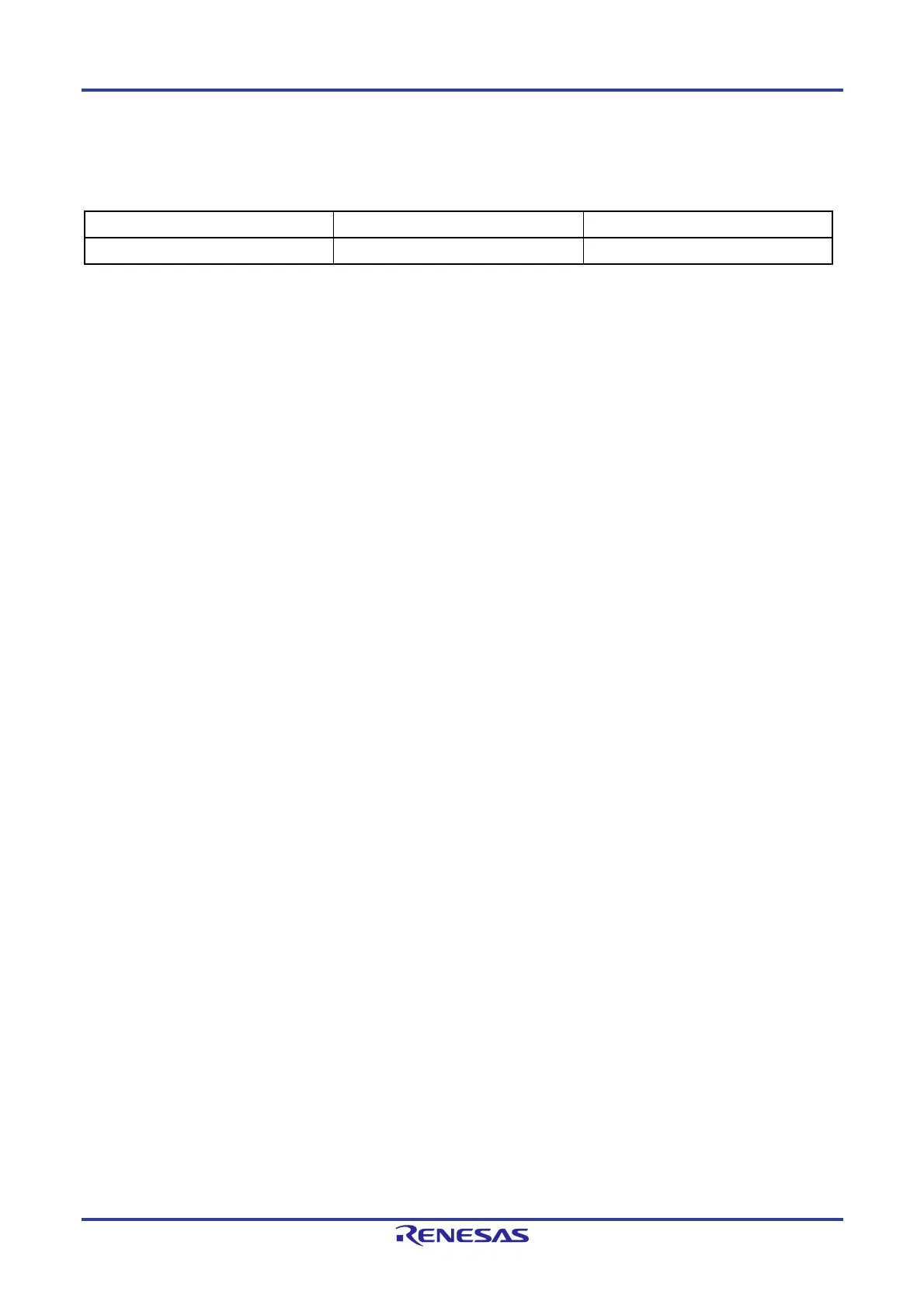
Whether the output pin for the clock and buzzer output controller is present depends on the product.
Output pin 20, 30, and 32-pin products 48, 64, 80, and 100-pin products
PCLBUZ0 ―
Caution Most of the following descriptions in this chapter use the 80-pin as an example.
10.1 Functions of Clock Output/Buzzer Output Controller
The clock output controller is intended for carrier output during remote controlled transmission and clock output for supply
to peripheral ICs.
Buzzer output is a function to output a square wave of buzzer frequency.
One pin can be used to output a clock or buzzer sound.
The PCLBUZ0 pin outputs a clock selected by clock output select register 0 (CKS0).
Figure 10-1 shows the block diagram of clock output/buzzer output controller.
Caution In the low-consumption RTC mode (when the RTCLPC bit of the operation speed mode control register
(OSMC) = 1), it is not possible to output the sub/low-speed on-chip oscillator select clock (f
SL) from the
PCLBUZ0 pin.
 Loading...


