RL78/F13, F14 CHAPTER 12 A/D CONVERTER
R01UH0368EJ0210 Rev.2.10 750
Dec 10, 2015
12.7.2 Setting up hardware trigger no-wait mode
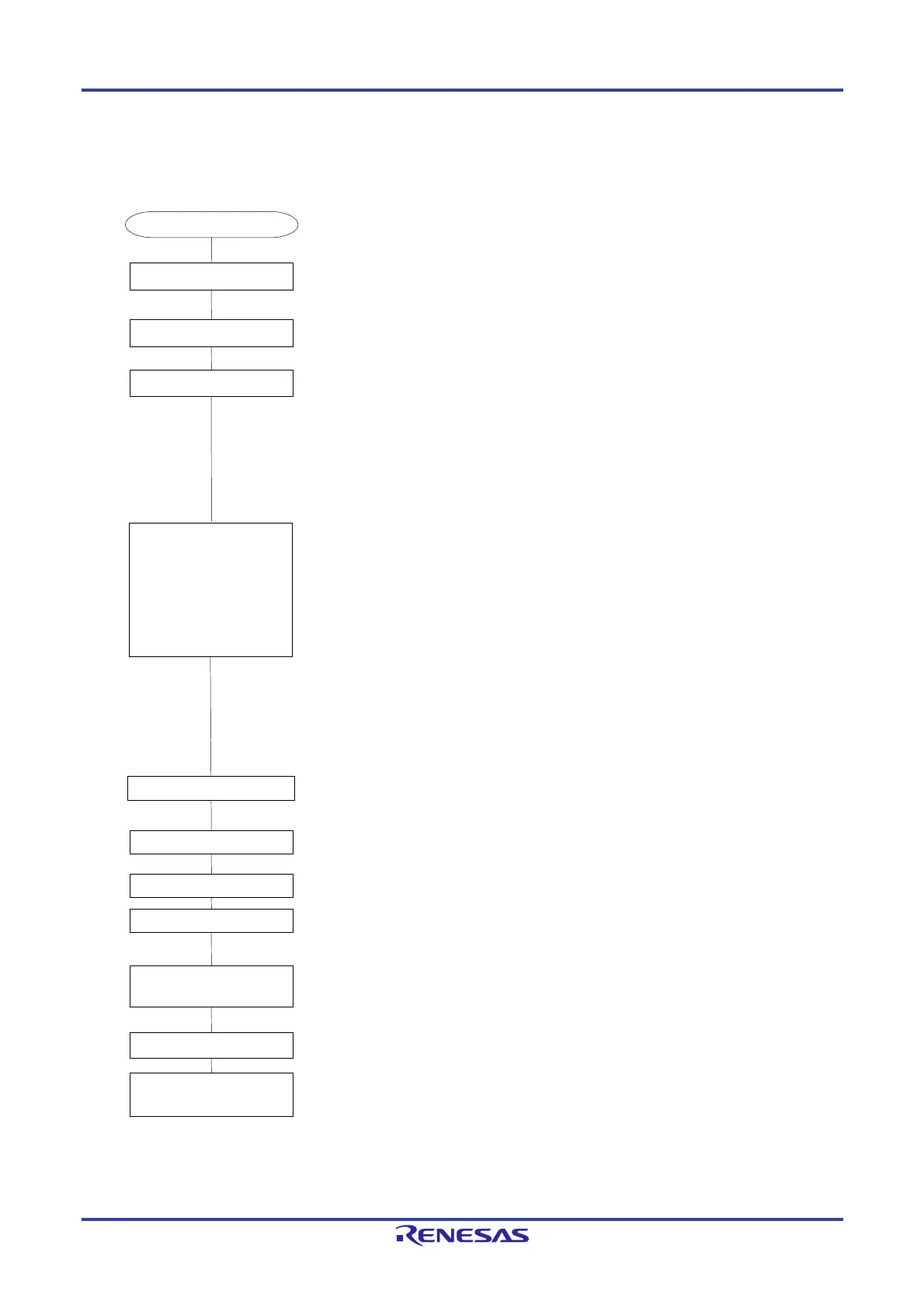
Figure 12-35. Setting up Hardware Trigger No-Wait Mode
Notes 1. Depends on the products.
2. Depending on the settings of the ADRCK bit and ADUL/ADLL registers, there is a possibility of no interrupt
signal being generated. In this case, the results are not stored in the ADCR and ADCRH registers.
Start of setup
PER0 register setting
ADPC and PMCxx register settings
PM register setting
• ADM0 register setting
• ADM1 register setting
• ADM2 register setting
• ADUL/ADLL register setting
• ADS register setting
(The order of the settings is
irrelevant.)
The ADCEN bit of the PER0 register is set (1), and supplying the clock starts.
The ports are set to analog input.
Note 1
ANI0 to ANI23 pins: Set using the ADPC register
ANI24 to ANI30 pins: Set using the PMCxx register
The ports are set to the input mode.
• ADM0 register
FR2 to FR0, LV1, and LV0 bits: These are used to specify the A/D conversion time.
ADMD bit: Select mode/scan mode
• ADM1 register
ADTMD1 and ADTMD0 bits: These are used to specify the hardware trigger no-wait
mode.
ADSCM bit: Sequential conversion mode/one-shot conversion mode
• ADM2 register
ADREFP1, ADREFP0, and ADREFM bits: These are used to select the reference
voltage source.
ADTYP bit: 8-bit/10-bit resolution
• ADUL/ADLL register
These are used to specify the upper limit and lower limit A/D conversion result
comparison values.
• ADS register
ADS4 to ADS0 bits: These are used to select the analog input channels.
ADCE bit setting
The ADCE bit of the ADM0 register is set (1), and the system enters the A/D conversion
standby status.
Stabilization w ait tim e count B
The software counts up to the stabilization wait time (1
µ
s).
Start of A/D conversion by
generating a hardware trigger
End of A/D conversion
The A/D conversion end interrupt (INTAD) is generated.
Note 2
Storage of conversion results in
the ADCR and ADCRH registers
The conversion results are stored in the ADCR and ADCRH registers.
ADCS bit setting
After counting up to the stabilization wait time B ends, the ADCS bit of the ADM0 register is
set (1), and the system enters the hardware trigger standby status.
Hardware trigger standby status
The A/D conversion operations are performed.
Stabilization wait time count A
ADRCK bit: This is used to select the range of values for comparison with the result of
A/D conversion in the generation of interrupt signals in response to results
being in either area 1 or areas 3 and 2.
Waiting for the time indicated by A below may be required for the results of conversion to become
stable after a change to the values of the ADREFP1 and ADREFP0 bits if the given condition holds.
If the values of ADREFP1 and ADREFP0 are changed to 1 and 0, respectively: A = 5 µs
A wait is not required if the values of ADREFP1 and ADREFP0 are changed to 0 and 0 or 0 and 1,
respectively.
 Loading...


