RL78/F13, F14 CHAPTER 35 ELECTRICAL SPECIFICATIONS (GRADE K)
R01UH0368EJ0210 Rev.2.10 1736
Dec 10, 2015
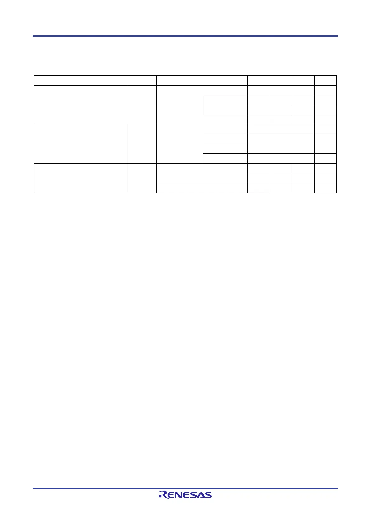
35.2.4 PLL Circuit Characteristics
(TA = -40 to +125C, 2.7 V EVDD0 = EVDD1 = VDD 5.5 V, VSS = EVSS0 = EVSS1 = 0 V)
Resonator Symbol Conditions MIN. TYP. MAX. Unit
PLL input enable clock frequency
Note 1
fPLLI PLLMUL = 0 PLLDIV0 = 0 3.92 4.0 4.08 MHz
PLLDIV0 = 1 7.84 8.0 8.16 MHz
PLLMUL = 1 PLLDIV0 = 0 3.92 4.0 4.08 MHz
PLLDIV0 = 1 7.84 8.0 8.16 MHz
PLL output frequency (center value) fPLL PLLMUL = 0 PLLDIV0 = 0 fPLLI × 12/2 MHz
PLLDIV0 = 1 fPLLI × 12/4 MHz
PLLMUL = 1
Note 4
PLLDIV0 = 0
Note 4
fPLLI × 16/2 MHz
PLLDIV0 = 1 fPLLI × 16/4 MHz
Long-term jitter
Notes 2, 3
tLJ fPLL = 24 MHz (480 counts) -2 +2 ns
fPLL = 32 MHz (640 counts) -2 +2 ns
fPLL = 48 MHz (960 counts) -2 +2 ns
Notes 1. If the high-speed on-chip oscillator clock is to be selected as the PLL input clock, the minimum and maximum
values will reflect the range of accuracy of the oscillation frequency by the high-speed on-chip oscillator clock.
2. Guaranteed by design, but not tested before shipment.
3. Indicates 20 µs.
4. Setting of PLLMUL = 1 and PLLDIV0 = 0 is prohibited when fPLLI > 6 MHz.
 Loading...


