RL78/F13, F14 CHAPTER 30 FLASH MEMORY
R01UH0368EJ0210 Rev.2.10 1626
Dec 10, 2015
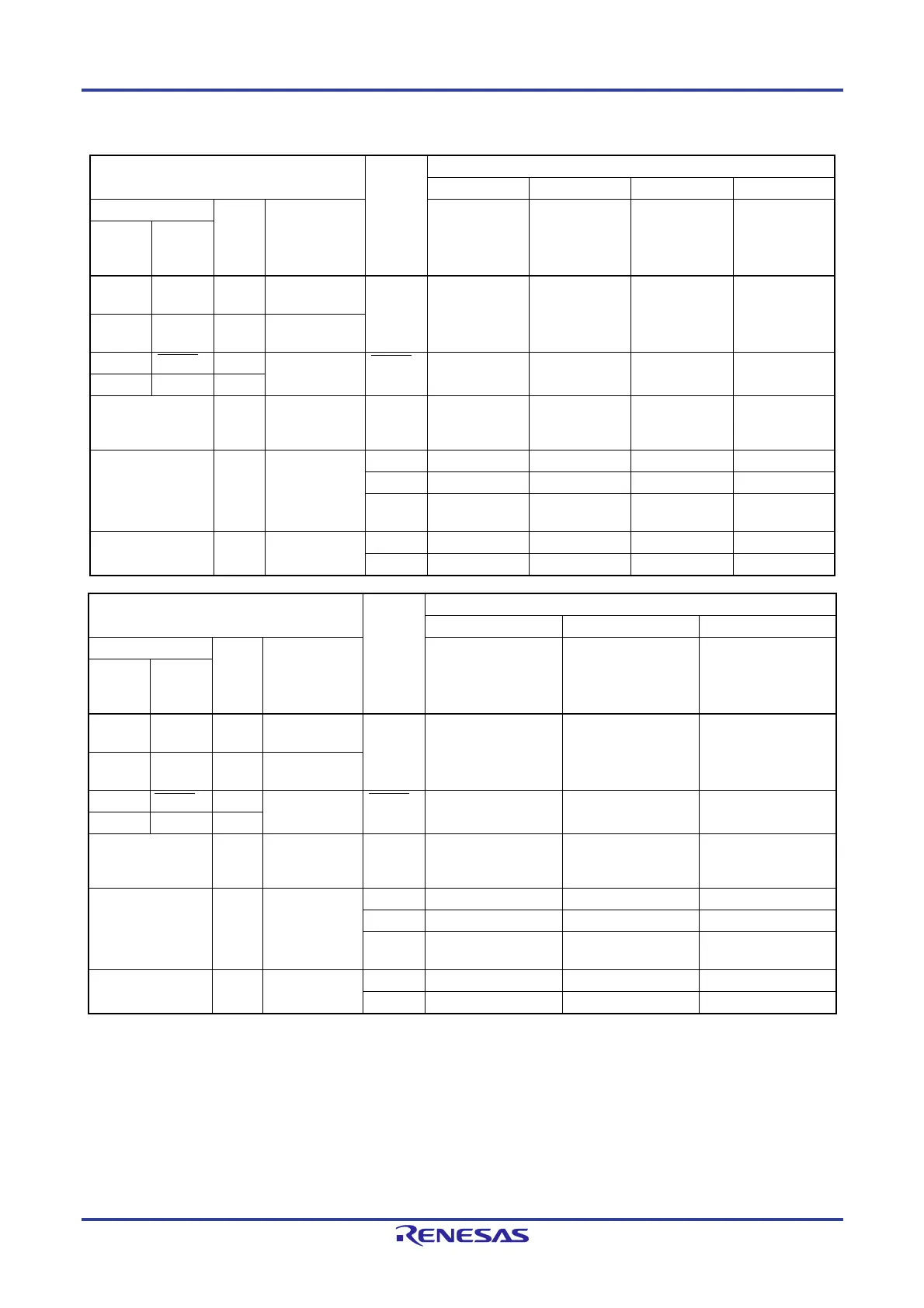
Table 30-1. Wiring Between the RL78/F13 or RL78/F14 and Dedicated Flash Memory Programmer
Pin Configuration of Dedicated Flash Memory
Programmer
Pin Name Pin No.
20-pin 30-pin 32-pin 48-pin
Signal Name I/O Pin Function SSOP SSOP
VQFN
(5x5)
LQFP (7x7),
VQFN (7x7)
PG-FP5,
FL-PR5
E1 on-chip
debugging
emulator
TOOL0 I/O
Transmit/receive
signal
TOOL0/
P40
3 8 3 3
SI/RxD I/O
Transmit/receive
signal
RESET Output Reset signal RESET 4 9 4 4
/RESET Output
VDD I/O
V
DD voltage
generation/
power monitoring
V
DD 10 15 10 12
GND Ground VSS 9 14 9 11
EVSS
REGC
Note
8 13 8 10
EMVDD
Driving power
for TOOL0 pin
VDD 10 15 10 12
EVDD
Pin Configuration of Dedicated Flash Memory
Programmer
Pin Name Pin No.
64-pin 80-pin 100-pin
Signal Name I/O Pin Function LQFP (10x10) LQFP (12x12) LQFP (14x14)
PG-FP5,
FL-PR5
E1 on-chip
debugging
emulator
TOOL0 I/O
Transmit/receive
signal
TOOL0/
P40
5 9 12
SI/RxD I/O
Transmit/receive
signal
RESET Output Reset signal RESET 6 10 13
/RESET Output
VDD I/O
V
DD voltage
generation/
power monitoring
V
DD 15 19 22
GND Ground VSS 13 17 20
EVSS 14 18 21, 43
REGC
Note
12 16 19
EMVDD
Driving power
for TOOL0 pin
VDD
EVDD 16 20 23, 53
Note Connect REGC pin to ground via a capacitor (0.47 to 1
F).
Remark Pins that are not indicated in the above table can be left open when using the flash memory programmer
for flash programming.
 Loading...


