RL78/F13, F14 CHAPTER 35 ELECTRICAL SPECIFICATIONS (GRADE K)
R01UH0368EJ0210 Rev.2.10 1740
Dec 10, 2015
(T
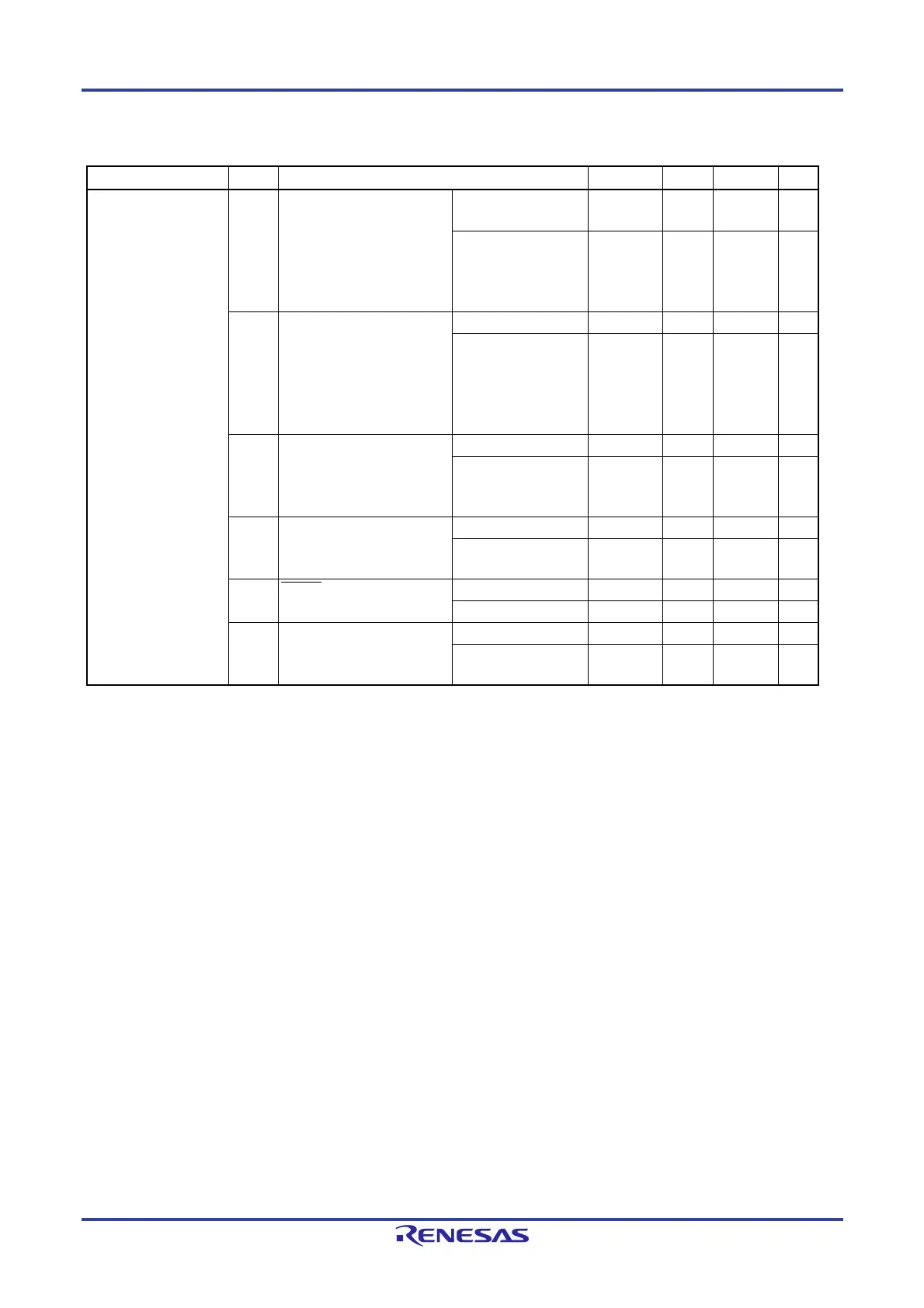
A = -40 to +125C, 2.7 V EVDD0 = EVDD1 = VDD 5.5 V, VSS = EVSS0 = EVSS1 = 0 V) (4/4)
Items Symbol Conditions MIN. TYP. MAX. Unit
Input voltage, low VIL1
P00 to P03, P10 to P17, P30
to P32, P40 to P47, P50 to
P57, P60 to P67, P70 to P77,
P106, P107, P120, P125 to
P127, P140, P150 to P157
(Schmitt 1 mode)
4.0 V EV
DD0 5.5 V
0
0.35
EV
DD0
V
2.7 V EVDD0 < 4.0 V 0
0.3 EVDD0 V
VIL2
P10, P11, P13, P14, P16,
P17, P30, P43, P50, P52 to
P54, P60 to P63, P70, P71,
P73, P75 to P77, P107, P125,
P150, P152, P153
(Schmitt 3 mode)
4.0 V EV
DD0 5.5 V
0
0.5 EVDD0 V
2.7 V EVDD0 < 4.0 V 0
0.4 EVDD0 V
VIL3
P10, P11, P13, P14, P16,
P17, P30, P54, P62, P63,
P70, P71, P73, P125
(TTL mode)
4.0 V EV
DD0 5.5 V
0 0.8 V
2.7 V EVDD0 < 4.0 V 0 0.5 V
VIL4
Note
P33, P34, P80 to P87, P90 to
P97, P100 to P105, P137
(fixed to Schmitt 3 mode)
4.0 V V
DD 5.5 V
0 0.5 VDD V
2.7 V VDD < 4.0 V 0 0.4 VDD V
VIL5 RESET
(fixed to Schmitt 1 mode)
4.0 V VDD 5.5 V
0 0.35 VDD V
2.7 V VDD < 4.0 V 0 0.3 VDD V
VIL6 P121 to P124, EXCLK,
EXCLKS
(fixed to Schmitt 2 mode)
4.0 V V
DD 5.5 V
0 0.2 VDD V
2.7 V VDD < 4.0 V 0 0.2 VDD V
Note P92 to P96 of the Group A products are fixed to Schmitt 1 mode.
P96 and P97 of the Group B, C, and D products are fixed to Schmitt 1 mode.
Remark Unless specified otherwise, the characteristics of alternate-function pins are the same as those of the port pins.
 Loading...


