EasyManuals Logo
Home>Renesas>Computer Hardware>RL78/D1A

Renesas RL78/D1A User Manual

Renesas RL78/D1A
1879 pages
To Next Page IconTo Next Page
To Previous Page IconTo Previous Page
Page #232 background imageLoading...
Page #232 background image
RL78/F13, F14 CHAPTER 3 CPU ARCHITECTURE
R01UH0368EJ0210 Rev.2.10 200
Dec 10, 2015
Figure 3-69. Example of RETI, RETB
RETI, RETB
SP
F0000H
PC
SP
PSW
Stack
area
Memory
SP+3 (SP+3)
(SP+2)
(SP+1)
(SP)
SP+2
SP+1
SP
SP+4
OP-code
<1>
<1>
Instruction code
<2>
<3>
Stack addressing is specified <1>.
The contents of addresses SP, SP + 1, SP + 2, and SP + 3 are
stored in PC bits 7 to 0, 15 to 8, 19 to 16, and the PSW, respectively
<2>.
The value of SP <3> is increased by four
.

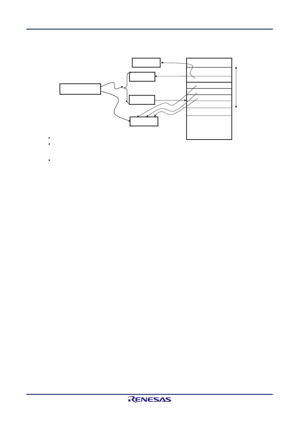
Table of Contents

Questions and Answers:

Question and Answer IconNeed help?

Do you have a question about the Renesas RL78/D1A and is the answer not in the manual?

Renesas RL78/D1A Specifications

General IconGeneral
BrandRenesas
ModelRL78/D1A
CategoryComputer Hardware
LanguageEnglish

Related product manuals