RL78/F13, F14 CHAPTER 12 A/D CONVERTER
R01UH0368EJ0210 Rev.2.10 732
Dec 10, 2015
The ANI0/P33 to ANI23/P105 pins are as shown below depending on the settings of the A/D port configuration register
(ADPC), analog input channel specification register (ADS), PM3, PM8, PM9, and PM10 registers.
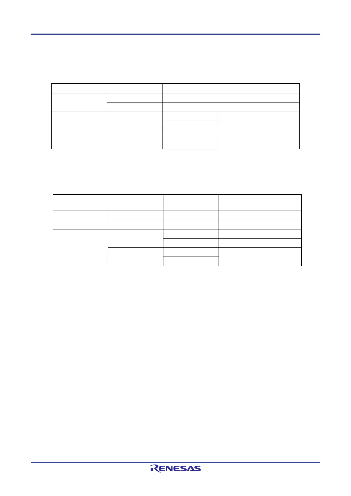
Table 12-4. Setting Functions of ANI0/P33 to ANI23/P105 Pins
ADPC PM3, PM8, PM9, PM10 ADS ANI0/P33 to ANI23/P105 Pins
Digital I/O selection Input mode
Digital input
Output mode
Digital output
Analog input selection Input mode Selects ANI. Analog input (to be converted)
Does not select ANI. Analog input (not to be converted)
Output mode Selects ANI. Setting prohibited
Does not select ANI.
The ANI24 to ANI30 pins are as shown below depending on the settings of port mode control registers 7, 9, and 12
(PMC7, PMC9, PMC12), analog input channel specification register (ADS), PM7, PM9, and PM12 registers.
Table 12-5. Setting Functions of ANI24 to ANI30 Pins
PMC7, PMC9, and
PMC12
PM7, PM9, and PM12 ADS ANI24 to ANI30 Pins
Digital I/O selection Input mode
Digital input
Output mode
Digital output
Analog input selection Input mode Selects ANI. Analog input (to be converted)
Does not select ANI. Analog input (not to be converted)
Output mode Selects ANI. Setting prohibited
Does not select ANI.
 Loading...


