RL78/F13, F14 CHAPTER 17 LIN/UART MODULE (RLIN3)
R01UH0368EJ0210 Rev.2.10 1210
Dec 10, 2015
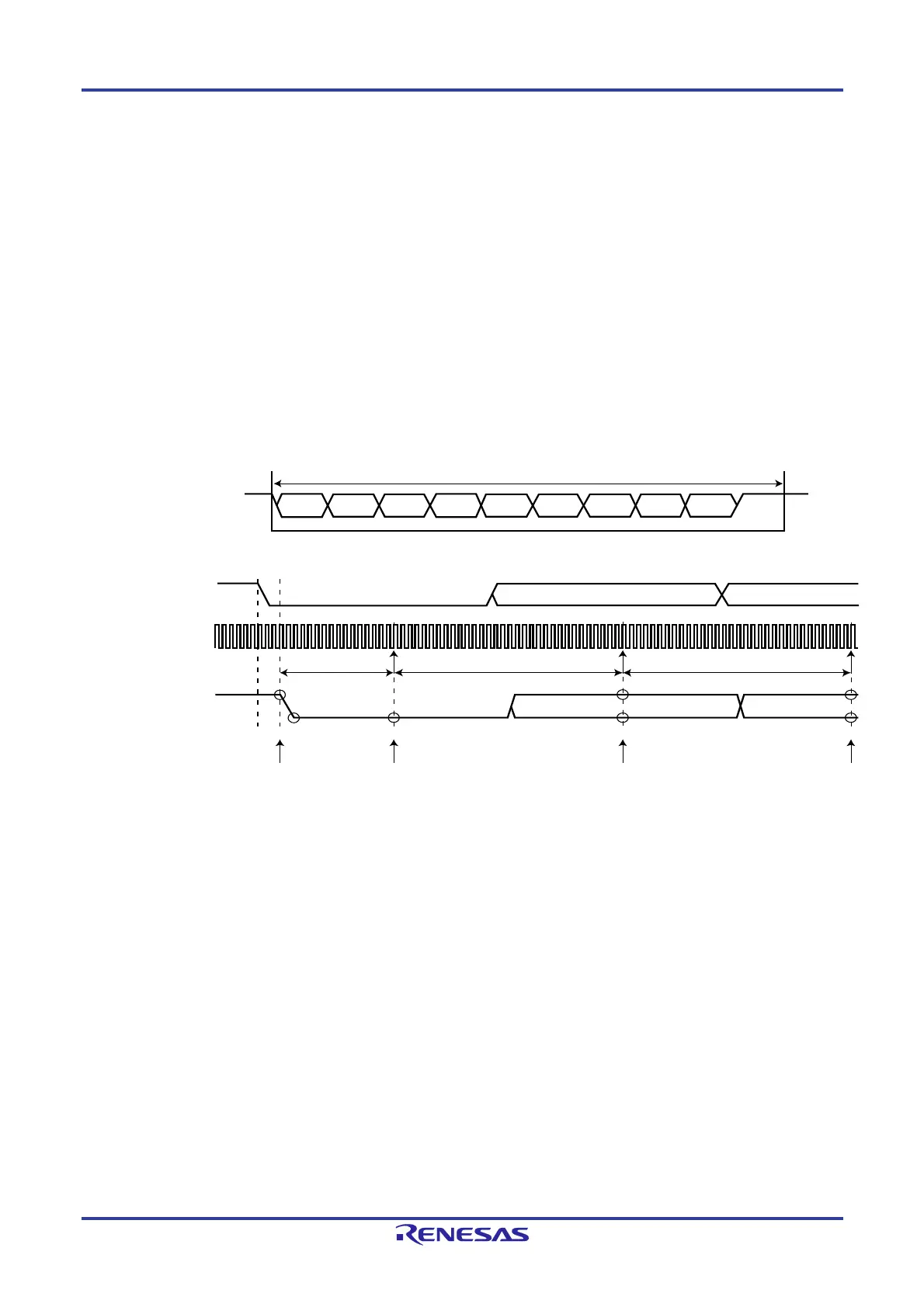
(2) Data Reception
Data reception is performed by using the synchronized LRXDn signal (an internal signal) that is the input from the LRXDn
pin synchronized with prescaler clock.
The byte field is synchronized at the falling edge of the start bit for the synchronized LRXDn signal. After the falling edge is
detected, sampling is performed again 0.5 Tbit later, and the falling edge is recognized as a start bit if the synchronized
LRXDn signal is low. The falling edge is not recognized as a start bit if the LRXDn signal after the clearing of the resetting is
low-fixed or if a high level is detected on re-sampling.
After the start bit is detected, the system samples 1 bit per Tbit.
The LIN/UART module has a noise filter function with respect to reception data. If the LRDNFS bit in the LMDn register is 0,
the LIN/UART module uses a noise filter, and for a sampling value the value determined by a 3-sampling majority rule on
prescaler clocks is used. If the LRDNFS bit in the LMDn register is 1, the LIN/UART module does not use a noise filter, and
for a sampling value the value of the synchronized LRXDn value at the sampling position is used as is.
Figure 17-15 shows an example of data reception timing.
Figure 17-15. Example of Data Reception Timing (LIN Master Mode, LIN Slave Mode [Fixed Baud Rate])
LRXDn
ST D0
D0 D1
D1 D2 D3 D4 D5 D6 D7 SP
Byte field
Data (8 bits)Start bit
Start bit
Start bit
LRXDn (Enlarged)
Prescaler clock
(internal signal)
Synchronized
LRXDn
(internal signal)
n = 0, 1
Falling
edge
detection
Confirmed to be low 0.5 Tbit
after falling edge detection.
0.5 Tbit 1 Tbit (= 16 f
LIN
)1 Tbit (= 16 f
LIN
)
D1D0
Bit 0 is read 1 Tbit after
confirmation of a low level.
After that, data bit is
read every Tbit.
Stop bit
 Loading...


