RL78/F13, F14 CHAPTER 30 FLASH MEMORY
R01UH0368EJ0210 Rev.2.10 1631
Dec 10, 2015
30.3 Connection of Pins on Board
To write the flash memory on-board by using the flash memory programmer, connectors that connect the dedicated flash
memory programmer must be provided on the target system. First provide a function that selects the normal operation mode
or flash memory programming mode on the board.
When the flash memory programming mode is set, all the pins not used for programming the flash memory are in the
same status as immediately after reset. Therefore, if the external device does not recognize the state immediately after
reset, the pins must be handled as described below.
Remark For flash programming mode, see 30.4.2 Flash memory programming mode.
30.3.1 P40/TOOL0 pin
In the flash memory programming mode, connect this pin to the dedicated flash memory programmer via an external
1 k pull-up resistor.
When this pin is used as the port pin, use that by the following method.
When used as an input pin: Input of low-level is prohibited for 1 ms period after the pin reset is released. However,
when this pin is used via pull-down resistors, use the 500 k or more resistors.
When used as an output pin: When this pin is used via pull-down resistors, use the 500 k or more resistors.
Remarks 1. t
HD: How long to keep the TOOL0 pin at the low level from when the external and internal resets end for
setting of the flash memory programming mode.
2. The SAU and IICA pins are not used for communication between the RL78/F13 or RL78/F14 and the
dedicated flash memory programmer, because single-line UART (TOOL0 pin) is used.
30.3.2 RESET pin
Signal conflict will occur if the reset signal of the dedicated flash memory programmer and external device are connected
to the RESET pin that is connected to the reset signal generator on the board. To prevent this conflict, isolate the connection
with the reset signal generator.
The flash memory will not be correctly programmed if the reset signal is input from the user system while the flash memory
programming mode is set. Do not input any signal other than the reset signal of the dedicated flash memory programmer
and external device.
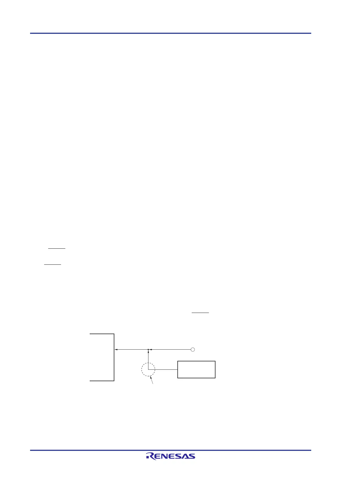
Figure 30-5. Signal Conflict (RESET Pin)
Input pin
Dedicated flash memory programmer
connection pin
Another device
Signal conflict
Output pin
In the flash memory programming mode, a signal output by another device
will conflict with the signal output by the dedicated flash memory
programmer. Therefore, isolate the signal of another device.
RL78/F13, RL78/F14
 Loading...


