RL78/F13, F14 CHAPTER 17 LIN/UART MODULE (RLIN3)
R01UH0368EJ0210 Rev.2.10 1209
Dec 10, 2015
17.4.2 Data Transmission/Reception
(1) Data Transmission
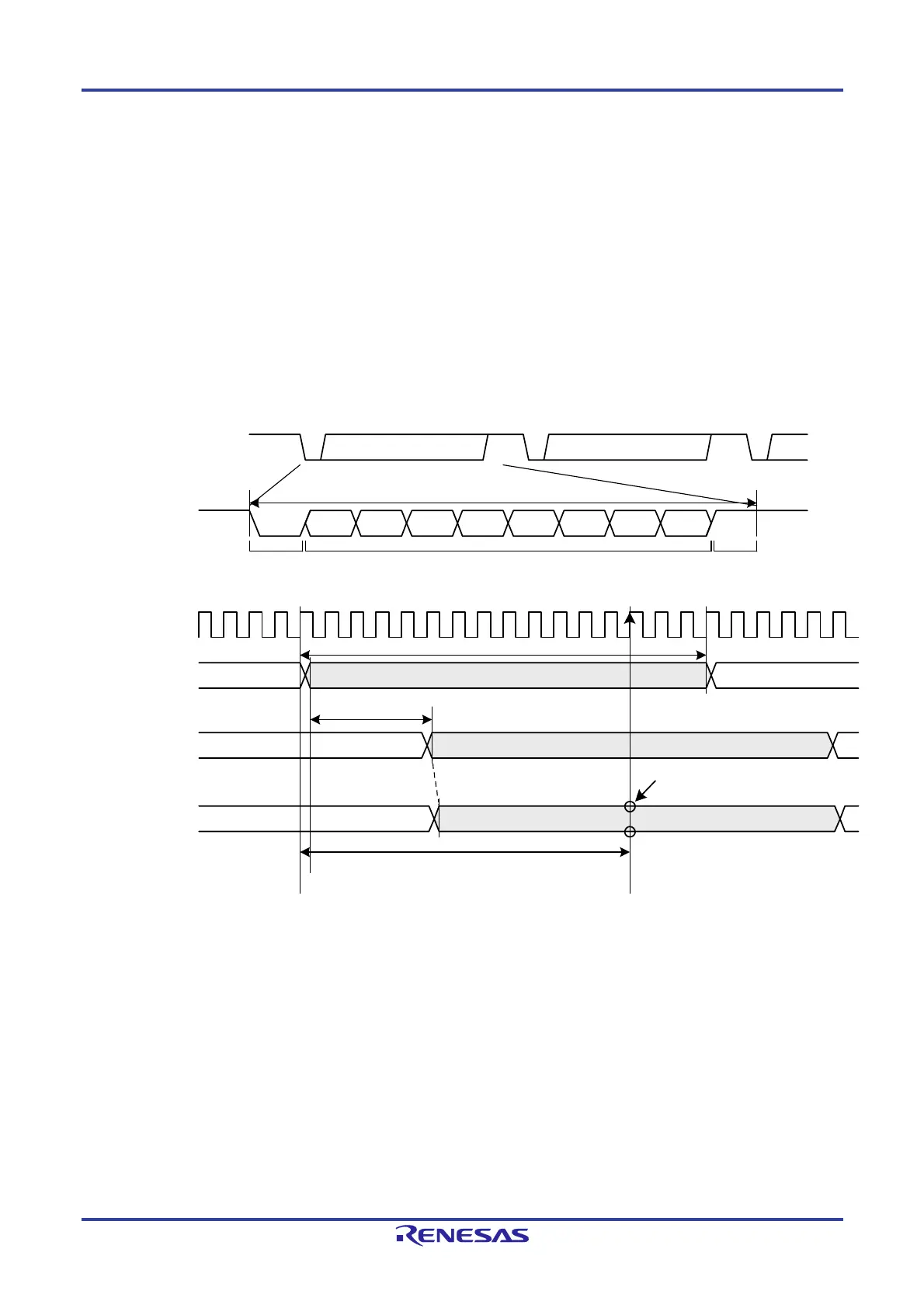
One bit of data is transmitted per 1 Tbit.
The data that is transmitted returns to the reception data input pin via the LIN transceiver. The received data and the
transmitted data is compared bit by bit, and the results are stored in the BER flag in the LESTn register (see 17.4.6 Error
Status).
In LIN master mode and LIN slave mode [fixed baud rate], 1 Tbit is generated to be 16fLIN, and thus the sampling point for
received data is at the 13th clock cycle (81.25% position).
In LIN slave mode [auto baud rate], if 1 Tbit is generated to be 4fLIN, the sampling point for received data is at the third
clock cycle (75% position). If 1 Tbit is generated to be 8fLIN, the sampling point for received data is at the 7th clock cycle
(87.5% position).
Figure 17-14 shows an example of data transmission timing.
Figure 17-14. Example of Data Transmission Timing (LIN Master Mode, LIN Slave Mode [Fixed Baud Rate])
ST
SPST
SP ST SP
D0 D1 D2 D3 D4 D5 D6 D7
DmDm-1
Dm-1 Dm
n = 0, 1
Dm-1 Dm
13/16Tbit
Synchronizing
LRXDn
f
LIN
(internal signal)
LTXDn
LRXDn
LTXDn
Start bit Data (8 bits)
Byte field
Data (8 bits)
Data (8 bits)
Stop bit
Physical layer delay
1 Tbit = 16 f
LIN
Sampling point for bit error detection
Dm+1
 Loading...


