RL78/F13, F14 CHAPTER 13 D/A CONVERTER (RL78/F14 Only)
R01UH0368EJ0210 Rev.2.10 764
Dec 10, 2015
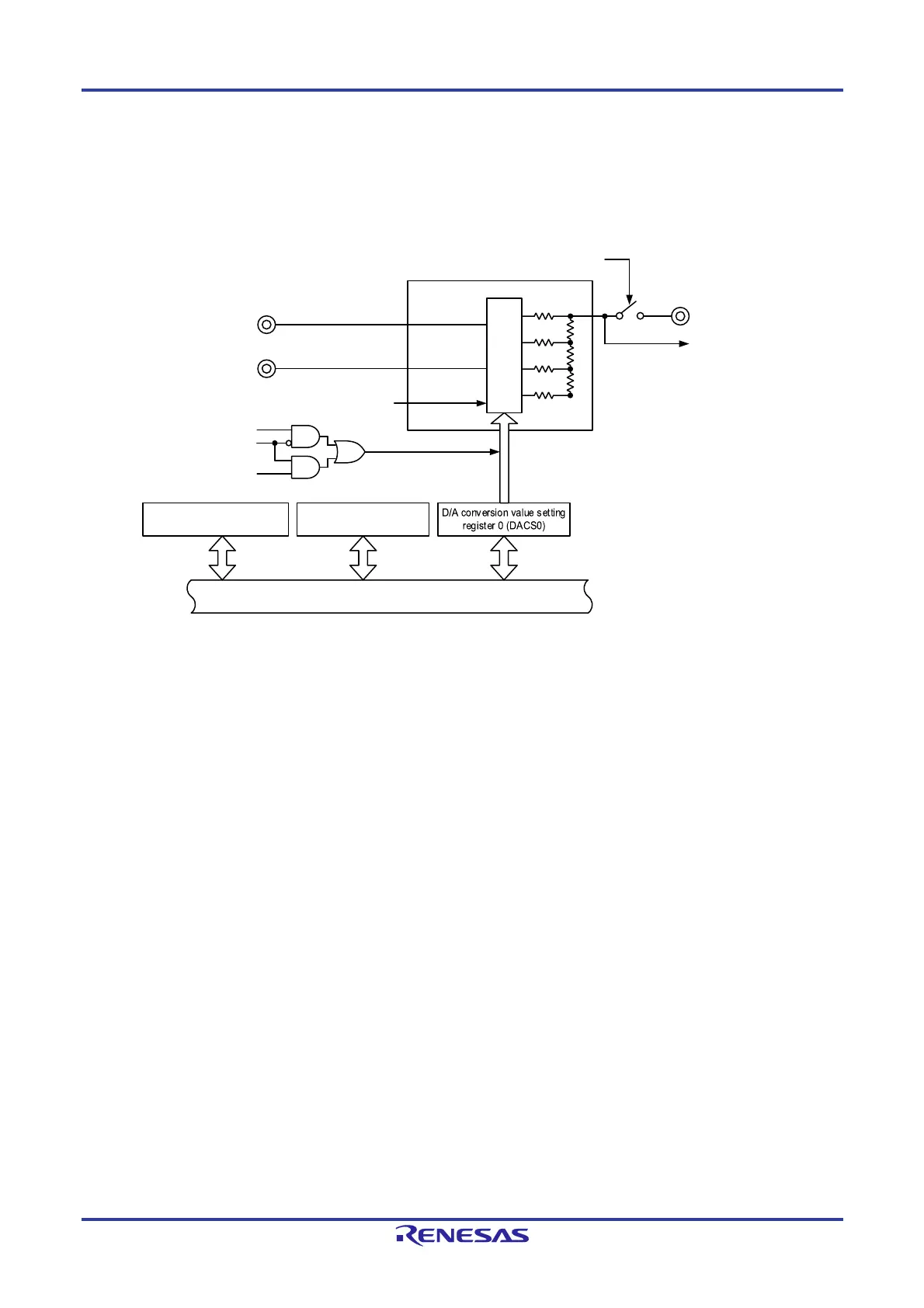
13.2 Configuration of D/A Converter
Figure 13-1 shows the block diagram of the D/A converter.
Figure 13-1. Block Diagram of D/A Converter
Remarks 1. ELCREQ0 is a trigger signal (request signal from the ELC) that is used in the real-time output mode.
2. The internal reference voltage (comparator) is used to select the reference voltage of the comparator. When
setting bits 5 and 4 (CVRS1 and CVRS0) in the comparator I/O select register (CMPSEL) to 10B (internal
reference voltage (DAC output) is selected), set the ANO0EN bit in this register to 0 (analog output is
disabled).
Write signal of DACS0 register
DAMD0 (DAM)
ELCREQ0
V
DD
pin
V
SS
pin
Selector
D/A converter mode
register (DAM)
Internal bus
DACE0 (DAM)
ANO0EN bit (DAM2)
D/A converter mode
register 2 (DAM2)
ANO0/P80/ANI2 pin
Internal reference voltage
(comparator)
 Loading...


