RL78/F13, F14 CHAPTER 7 TIMER RJ
R01UH0368EJ0210 Rev.2.10 554
Dec 10, 2015
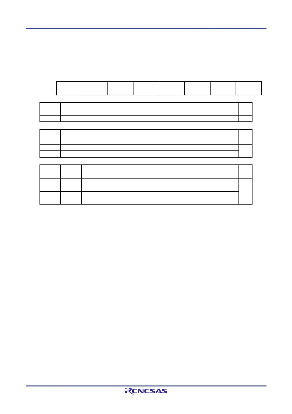
7.3.8 Timer RJ Event Pin Select Register 0 (TRJISR0)
Figure 7-9. Format of Timer RJ Event Pin Select Register 0 (TRJISR0)
Address : F0243H After Reset: 00H
Symbol 7 6 5 4 3 2 1 0
TRJISR0 —
— — — —
RCCPSEL2
Note
RCCPSEL1
Note
RCCPSEL0
Note
Bit 7 to
3
Nothing is assigned R/W
— The write value must be 0. The read value is 0. R
RCCPS
EL2
Timer output signal and INTP4 polarity selection
R/W
0 An event is counted during the low-level period R/W
1 An event is counted during the high-level period
RCCPS
EL1
RCCPS
EL0
Timer output signal selection R/W
0 0 TRDIOD1 R/W
0 1 TRDIOC1
1 0 TO02
1 1 TO03
Note Bits RCCPSEL0 to RCCPSEL2 are enabled only in event counter mode.
Caution The 20-pin products do not have the timer RJ event pin select register 0 (TRJISR0).
 Loading...


