RL78/F13, F14 CHAPTER 18 CAN INTERFACE (RS-CAN LITE)
R01UH0368EJ0210 Rev.2.10 1423
Dec 10, 2015
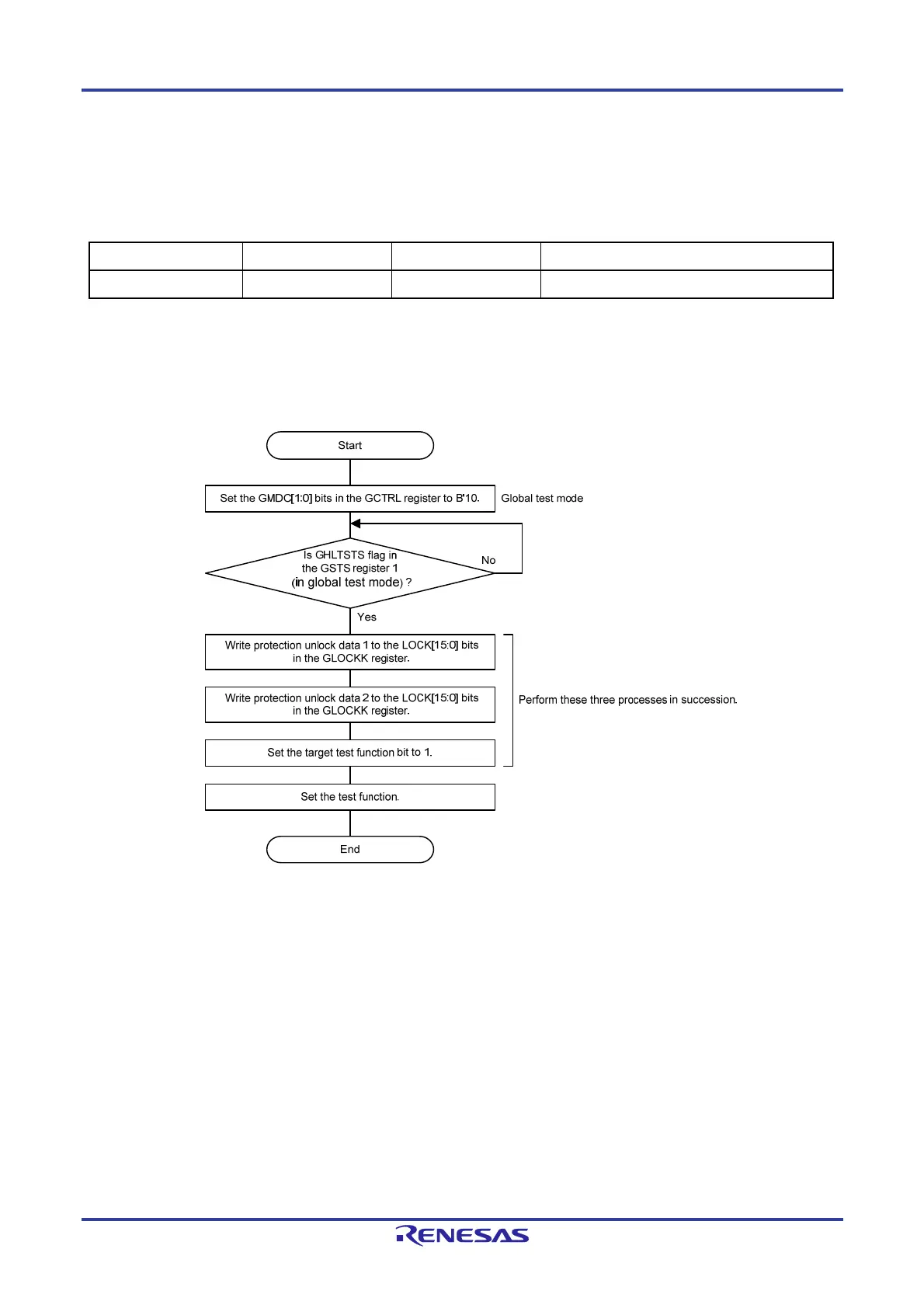
18.13.2 Protection Unlock Procedure
Since the global test functions shown in Table 18-15 are protected, write unlock data 1 and unlock data 2 in succession
to the LOCK[15:0] bits in the GLOCKK register, and then set each test function bit to 1.
Table 18-15. Protection Unlock Data for Test Functions
Test Function Protection Unlock Data 1 Protection Unlock Data 2 Target Bit
RAM test H'7575 H'8A8A RTME bit in the GTSTCTRL register
If an incorrect value has been written to the LOCK[15:0] bits, retry the procedure above from writing of unlock data 1.
Figure 18-34 shows the protection unlock procedure.
Figure 18-34. Protection Unlock Procedure
 Loading...


