RL78/F13, F14 CHAPTER 7 TIMER RJ
R01UH0368EJ0210 Rev.2.10 545
Dec 10, 2015
7.3 Registers
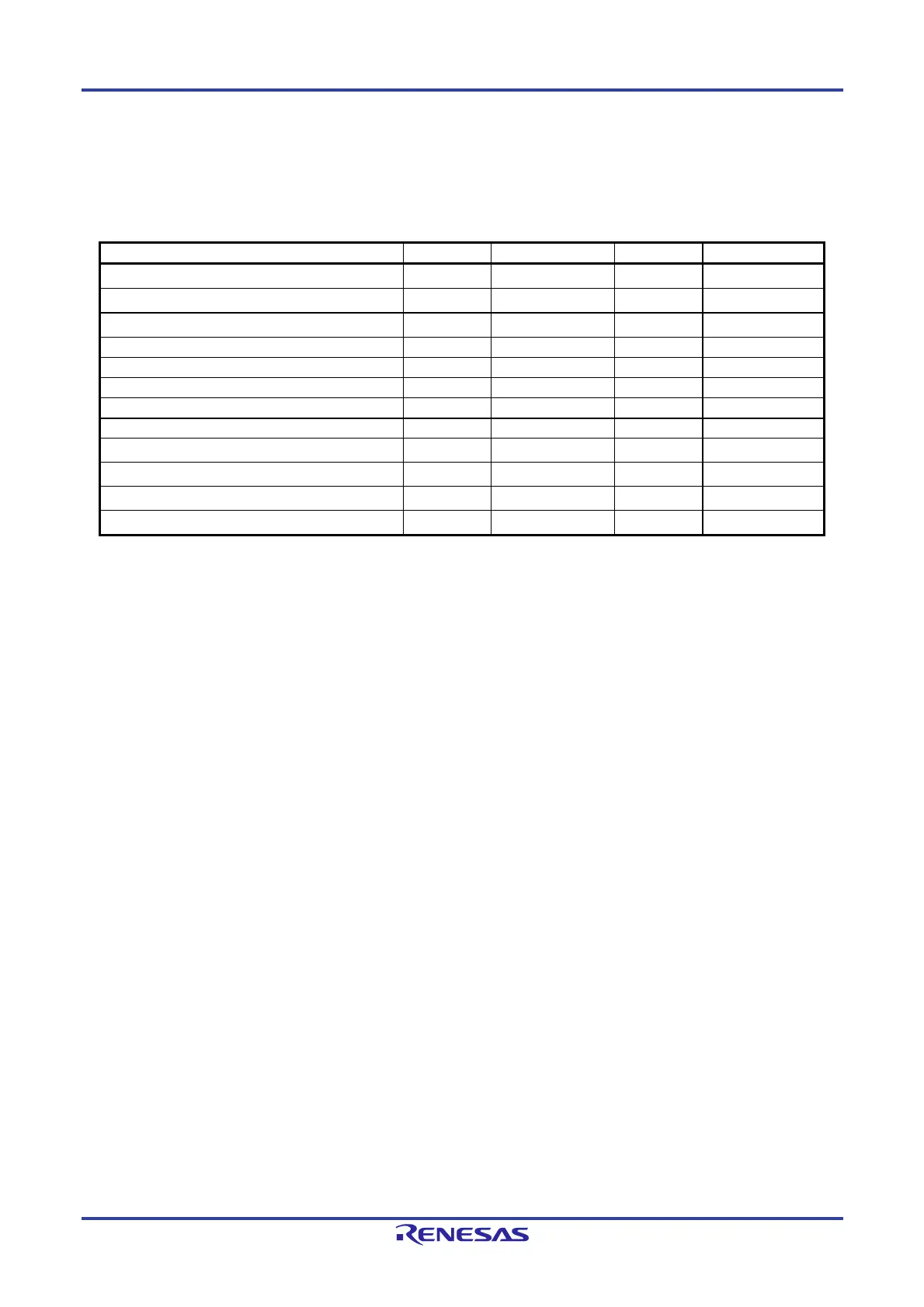
Table 7-3 lists the Timer RJ Register Configuration.
Table 7-3. Timer RJ Register Configuration
Register Name Symbol After Reset Address Access Size
Peripheral Enable Register 1 PER1 00H F02C0H 1, 8
Operation speed mode control register OSMC 00H F00F3H 8
Clock select register CKSEL 00H F02C4H 1, 8
Timer RJ Counter Register 0
Note 1
TRJ0 FFFFH F06F0H 16
Timer RJ Control Register 0 TRJCR0 00H F0240H 8
Timer RJ I/O Control Register 0
Note 2
TRJIOC0 00H F0241H 1, 8
Timer RJ Mode Register 0 TRJMR0 00H F0242H 8
Timer RJ Event Pin Select Register 0
Note 2
TRJISR0 00H F0243H 8
Port Register 1 P1 00H FFF01H 8
Port Register 4 P4 00H FFF04H 8
Port Mode Register 1
PM1 FFH FFF21H 8
Port Mode Register 4
PM4 FFH FFF24H 8
Notes 1. When the TRJ0 register is accessed, the CPU does not proceed to the next instruction processing but enters
the wait state for CPU processing. For this reason, if this wait state occurs, the number of instruction execution
clocks is increased by the number of wait clocks. The number of wait clocks for access to the TRJ0 register is
one clock for both writing and reading.
2. The 20-pin products do not have the timer RJ I/O control register 0 (TRJIOC0) and timer RJ event pin select
register 0 (TRJISR0).
 Loading...


