RL78/F13, F14 CHAPTER 19 DTC
R01UH0368EJ0210 Rev.2.10 1464
Dec 10, 2015
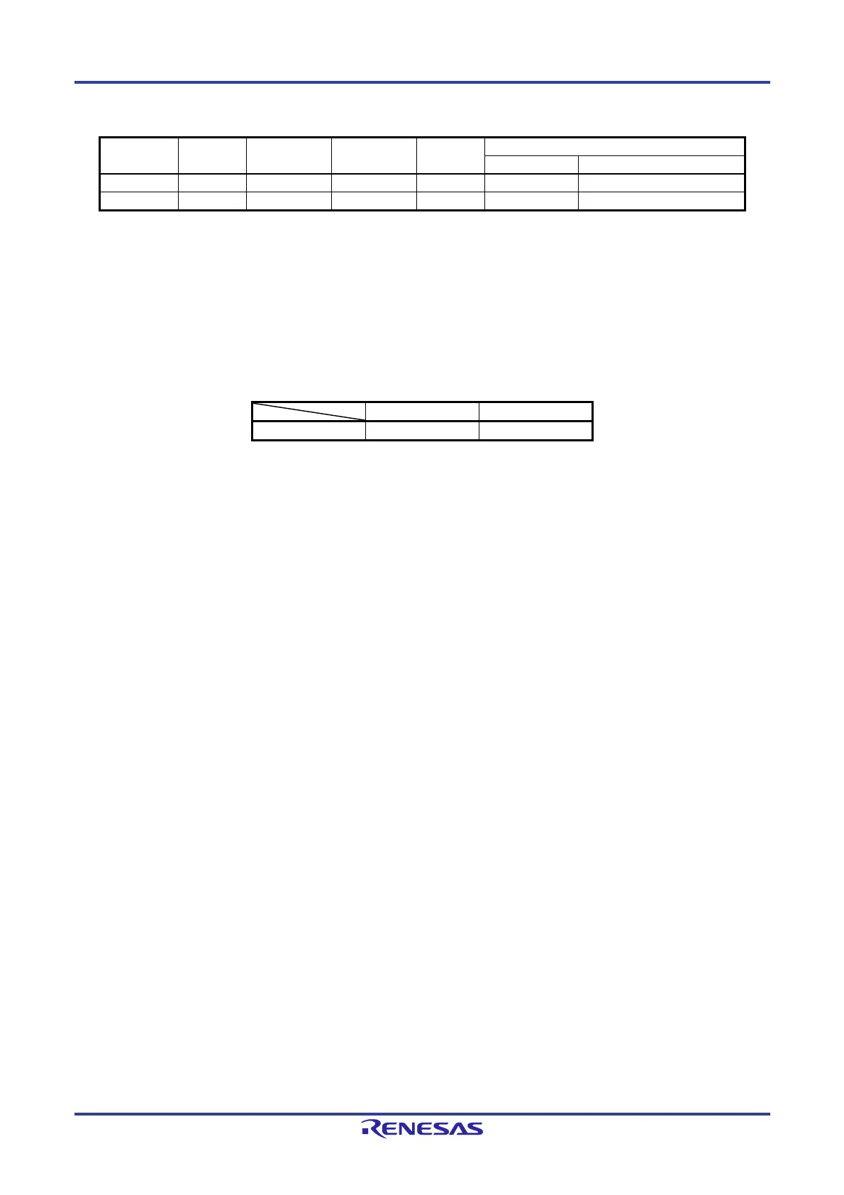
Table 19-15. Number of Clock Cycles Required for Data Read/Write Operation
Operation RAM Code Flash
Memory
Data Flash
Memory
SFR 2nd SFR
No Wait State Wait States
Data read - - - 1 1 1 + number of wait states
Note
Data write 1 - - 1 1 1 + number of wait states
Note
Note The number of wait states differs depending on the specifications of the register allocated to the second SFR to
be accessed.
19.4.8 DTC Response Time
Table 19-16 lists the DTC response time. The DTC response time is the time from when the DTC activation source is
detected until DTC transfer starts, excluding the number of DTC execution clocks.
The DTC response time in high-speed transfer is the same as that in the normal transfer.
Table 19-16. DTC Response Time
Minimum Time Maximum Time
Response Time 3 clocks 19 clocks
Note that the response from the DTC may be further delayed under the following cases. The number of delayed clock
cycles differs depending on the conditions.
When executing an instruction from the internal RAM
Maximum response time: 20 clocks
When executing a DTC pending instruction (refer to 19.4.3 DTC Pending Instruction)
Maximum response time: Maximum response time for each condition + execution clock cycles for the instruction to
be held pending under the condition.
When accessing the TRJ0 register that a wait occurs
Maximum response time: Maximum response time for each condition + 1 clock
Remark 1 clock: 1/f
CLK (fCLK: CPU/peripheral hardware clock)
19.4.9 DTC Activation Sources
After inputting a DTC activation source, do not input the same activation source again until DTC transfer is completed.
While a DTC activation source is generated, do not manipulate the DTC activation enable bit corresponding to the
source.
If DTC activation sources conflict, their priority levels are determined in order to select the source for activation when
the CPU acknowledges the DTC transfer. For details on the priority levels of activation sources, refer to 19.2.3 DTC
Vector Table.
When DTC activation is enabled under either of the following conditions, a DTC transfer is started and an interrupt is
generated after completion of the transfer. Therefore, enable DTC activation after confirming the comparator output
monitor flag (CMPMON0) as necessary.
- The comparator is set to releasing STOP mode by comparator interrupt enabled (CSTEN = 1), comparator output
not inverted (CINV = 0), and comparator input > reference voltage
- The comparator is set to releasing STOP mode by comparator interrupt enabled (CSTEN = 1), comparator output
inverted (CINV = 1), and comparator input < reference voltage
 Loading...


