RL78/F13, F14 CHAPTER 18 CAN INTERFACE (RS-CAN LITE)
R01UH0368EJ0210 Rev.2.10 1413
Dec 10, 2015
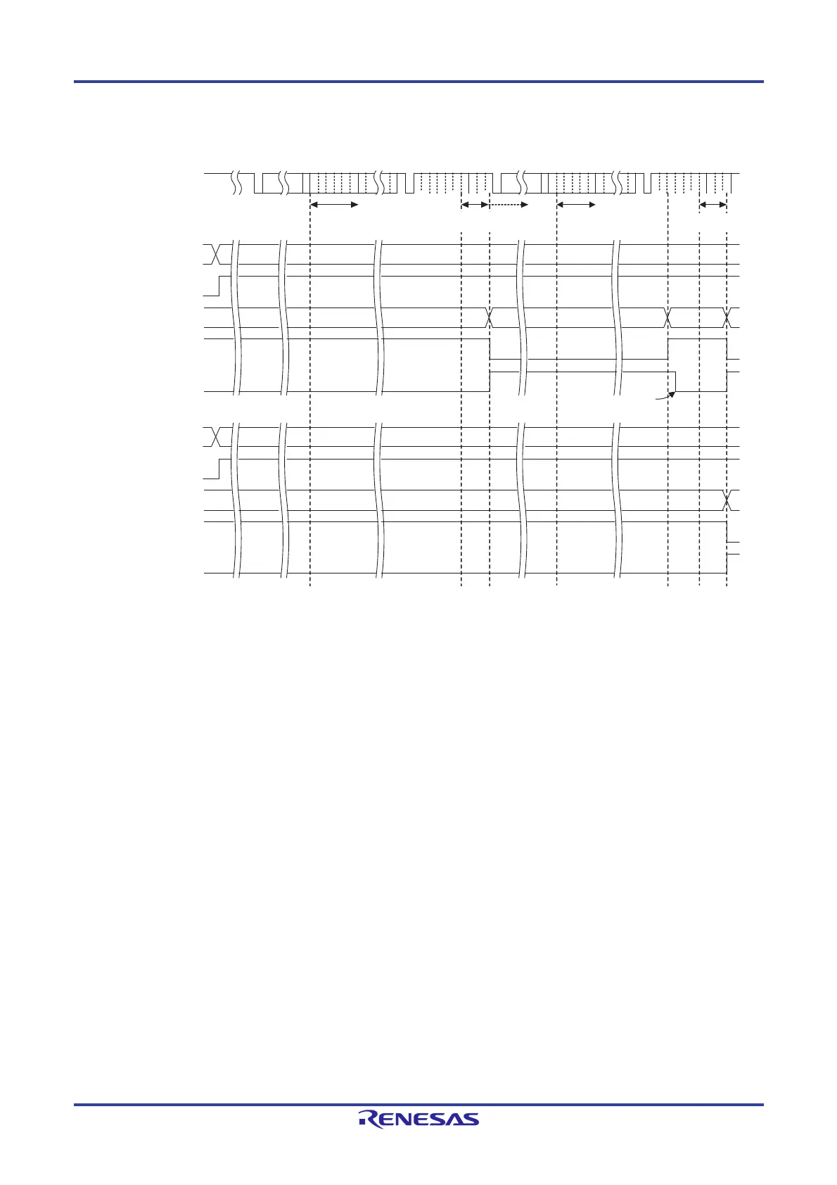
Figure 18-25. FIFO Buffer Reception Timing Chart
(1) When the ID field in a message has been received, the acceptance filter processing starts.
(2) When the message matches the receive rule of the corresponding channel and the message has been successfully
received, the routing processing to transfer the message to the specified buffer starts. When the DCE bit in the
GCFGL register is set to 1 (DLC check is enabled), the DLC filter processing starts at this time.
(3) When the message has passed through the DLC filter processing and the CFE value in the CFCCLk register is 1
(transmit/receive FIFO buffers are used) and the CFDC[2:0] value in the CFCCLk register is B'001 or more, the
message is stored in the transmit/receive FIFO buffer that is set to receive mode. The CFMC[5:0] value in the
CFSTSk register is incremented and becomes H'01. When the CFIM bit in the CFCCLk register is set to 1 (a FIFO
receive interrupt request is generated each time a message has been received), the CFRXIF flag in the CFSTSk
register is set to 1 (a transmit/receive FIFO receive interrupt request is present). The CFRXIF flag can be reset to 0
by the program.
(4) When the ID field of the next message has been received, the acceptance filter processing starts.
(5) Read received messages from the CFIDLk, CFIDHk, CFTSk, CFPTRk, and CFDF0k to CFDF3k registers and write
H'FF to the CFPCTRk register. Thereby the CFMC[5:0] bits in the CFSTSk register are decremented and become
H'00, and the CFEMP flag in the CFSTSk register becomes 1 (the transmit/receive FIFO buffer contains no
message (buffer empty)).
(6) When the message matches the receive rule of the corresponding channel and the message has been successfully
received, the routing processing to transfer the message to the specified buffer starts. When the DCE bit in the
GCFGL register is set to 1 (DLC check is enabled), the DLC filter processing starts at this time.
(1) (2) (3) (4)
SOF
ID
ACK
EOF
INT
SOF ACK
EOF
INT
ID
(6) (7)
0 1
(5)
101
0
0 3
1
0
H
L
1
0
1
0
1
0
1
0
1
0
1
0
CAN bus
[Transmit/receive FIFO buffer (receive mode)]
CFDC[2:0] bits
CFE bit
CFMC[5:0] bits
CFEMP flag
CFRXIF flag
[Receive FIFO buffer]
RFDC[2:0] bits
RFE bit
RFMC[5:0] bits
RFEMP flag
RFIF flag
k = 0, m = 0, 1
CFDC[2:0], CFE: Bits in the CFCCLk register
CFMC[5:0], CFEMP, CFRXIF: Flags in the CFSTSk register
RFDC[2:0], RFE: Bits in the RFCCm register
RFMC[5:0], RFEMP, RFIF: Flags in the RFSTSm register
CRC
delimiter
Cleared by the program
Acceptance
filter processing
Acceptance
filter processing
Routing and storage
processing
Routing and storage
processing
Control
Control
Remark
 Loading...


