RL78/F13, F14 CHAPTER 27 SAFETY FUNCTIONS
R01UH0368EJ0210 Rev.2.10 1606
Dec 10, 2015
<Control register>
Timer input select register 0 (TIS0)
This register is used to select the timer input of channel 1.
By selecting the low-speed on-chip oscillator clock for the timer input, its pulse width can be measured to determine
whether the proportional relationship between the low-speed on-chip oscillator clock and the timer operation clock is
correct.
The TIS0 register can be set by an 8-bit memory manipulation instruction.
Reset signal generation clears this register to 00H.
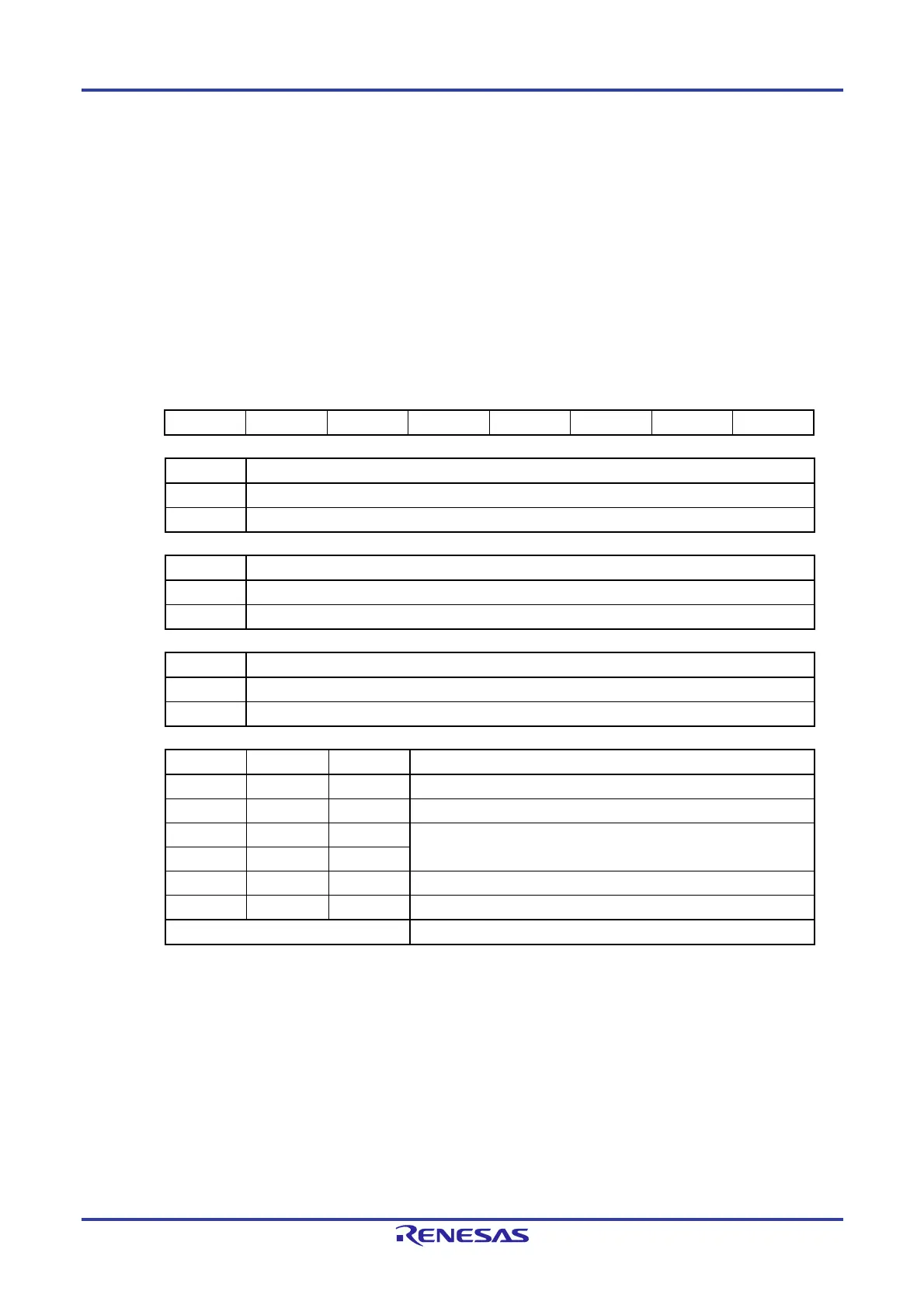
Figure 27-24. Format of Timer Input Select Register 0 (TIS0)
Address: F0074H After reset: 00H R/W
Symbol 7 6 5 4 3 2 1 0
TIS0 TIS07
Note 1
TIS06
Note 1
0 TIS04
Note 2
0 TIS02 TIS01 TIS00
TIS07
Note 1
Selection of timer input used with channel 3 of timer array unit 0
0 Input signal of timer input pin (TI03)
1 Event input signal from ELC
Note 3
TIS06
Note 1
Selection of timer input used with channel 2 of timer array unit 0
0 Input signal of timer input pin (TI02)
1 Event input signal from ELC
Note 3
TIS04
Note 2
Selection of timer input used with channel 0 of timer array unit 0
0 Input signal of timer input pin (TI00)
1 Event input signal from ELC
Note 3
TIS02 TIS01 TIS00 Selection of timer input used with channel 1 of timer array unit 0
0 0 0 Input signal of timer input pin (TI01)
0 0 1 Event input signal from ELC
Note 3
0 1 0 Input signal of timer input pin (TI01)
0 1 1
1 0 0 Low-speed on-chip oscillator clock (fIL)
1 0 1 Sub/low-speed on-chip oscillator select clock (fSL)
Other than above Setting prohibited
Notes 1. Provided only in products of group E. When writing data to the timer input select register 0 (TIS0)
of other products, always write 0.
2. Provided only in products of groups D and E. When writing data to the timer input select register 0
(TIS0) of other products, always write 0.
3. Provided only in products of groups D and E. Do not set a value for any other products.
(Cautions are provided on the next page.)
 Loading...


