RL78/F13, F14 CHAPTER 8 TIMER RD
R01UH0368EJ0210 Rev.2.10 635
Dec 10, 2015
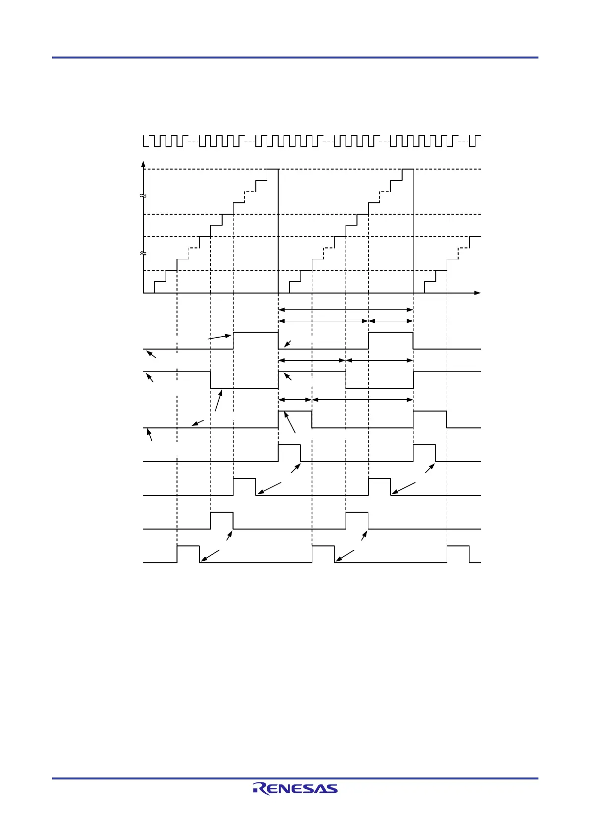
(1) Operation Example
Figure 8-53. Operation Example in PWM Function
m
n
p
Value in TRDi register
Count source
m + 1
n + 1
TRDIOCi output
q
m - n
p + 1 m - p
m - qq + 1
TRDIODi output
m: Value set in TRDG RA i register
n: Value set in TRDGRBi register
p: Value set in TRDGRCi register
q: Value set in TRDGRDi register
Inactive level is lowActive level is high
Inactive level is high
Act ive level is lo w
Initial output is low
until compare match
Initial output is low
until compare match
Set to 0 by a program Set to 0 by a program
Set to 0 by a program Set to 0 by a program
TRDIOBi output
IMFA bit in
TRDSRi register
IMFB bit in
TRDSRi register
IMFC bit in
TRDSRi register
IMFD bit in
TRDSRi register
Remark
i = 0 or 1
Initial output is high
until compare match
0000H Time
Inactive level is high
The above diagram applies under the following conditions:
Bits TRDBFCi and TRDBFDi in the TRDMR register are set t o 0 (TRDGRCi and TRDGRDi do not operate as buffers).
Bits EBi, ECi and EDi in the TRDOER1 regist er are set to 0 (TRDIOBi, TRDIOCi and TRDIODi output enabled).
Bits TOBi and TOCi in the TRDOCR register are set to 0 (inactive level), the TODi bit is set to 1 (active level).
The PO LB bit in the TRDPOCRi register is set to 1 (active level is high), bits POLC and POLD are set to 0 (active level is low).
 Loading...


