RL78/F13, F14 CHAPTER 12 A/D CONVERTER
R01UH0368EJ0210 Rev.2.10 760
Dec 10, 2015
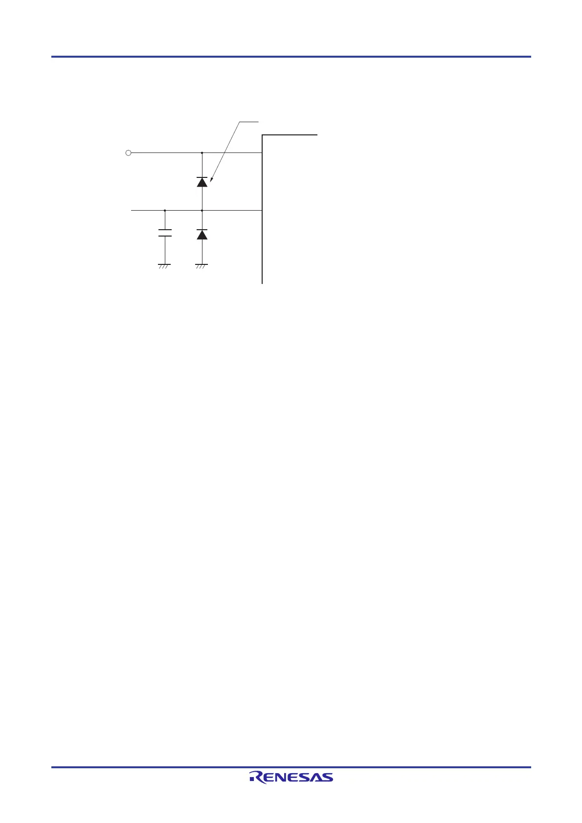
Figure 12-48. Analog Input Pin Connection
(5) Analog input (ANIn) pins
<1> The analog input pins (ANI0 to ANI23, ANI24 to ANI30) are also used as input port pins (P33, P34, P70 to P74,
P80 to P87, P90 to P97, P100 to P105, P120, P125).
Do not change the output values for the port-pin functions P33, P34, P70 to P74, P80 to P87, P90 to P97, P100
to P105, P120, and P125 while A/D conversion of the signals on the ANI0 to ANI23 or ANI24 to ANI30 pins is
selected and conversion is in progress, since doing so may lower the precision of the results of conversion.
<2> When a pin adjacent to one on which A/D conversion is in progress is used as a digital I/O port pin, coupling may
lead to noise that causes the results of A/D conversion to differ from the expected values. Be sure to prevent the
input or output of pulses on such pins while conversion is in progress.
(6) Input impedance of analog input (ANIn) pins
This A/D converter charges a sampling capacitor for sampling during sampling time.
Therefore, only a leakage current flows when sampling is not in progress, and a current that charges the capacitor flows
during sampling. Consequently, the input impedance fluctuates depending on whether sampling is in progress, and on
the other states.
To make sure that sampling is effective, however, it is recommended to keep the output impedance of the analog input
source to within 1 k, and to connect a capacitor of about 100 pF to the ANI0 to ANI23 and ANI24 to ANI30 pins (see
Figure 12-48).
AV
REFP
or V
DD
ANI0 to ANI23, ANI24 to ANI30
Reference
voltage
input
C = 100 to 1,000 pF
If there is a possibility that noise equal to or higher than AV
REFP
and
V
DD
or equal to or lower than AV
REFM
and V
SS
may enter, clamp with
a diode with a small V
F
value (0.3 V or lower).
 Loading...


