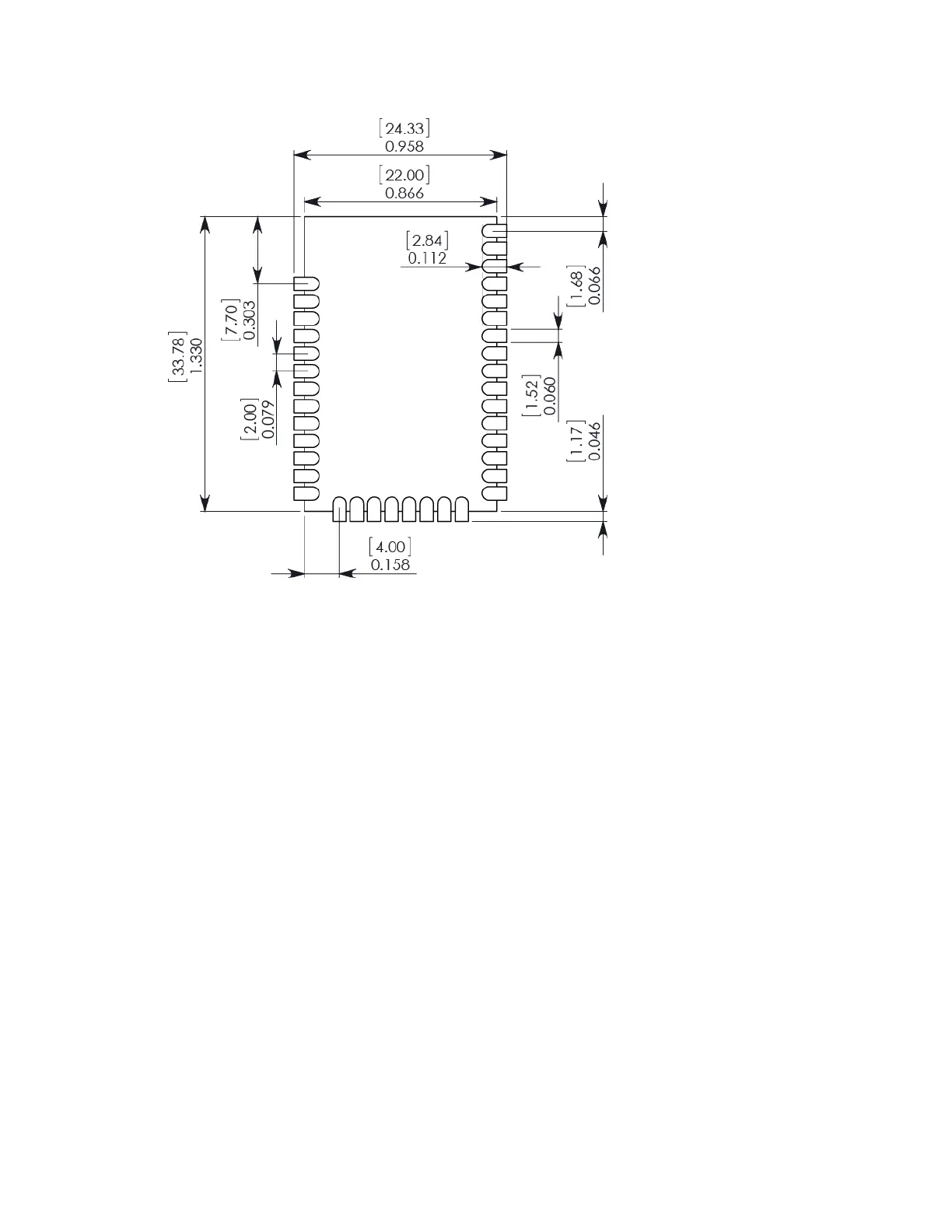
Manufacturing information Recommended footprint
XBee/XBee-PRO® S2C ZigBee® RF Module
301
Match the solder footprint to the copper pads, but may need to be adjusted depending on the specific
needs of assembly and product standards. Recommended stencil thickness is 0.15 mm/0.005”. Place
the component last and set the placement speed to the slowest setting.
While the underside of the device is mostly coated with solder resist, we recommended the copper
layer directly below the device be left open to avoid unintended contacts. Copper or vias must not
interfere with the three exposed RF test points on the bottom of the device as shown in the following
diagram. These devices have a ground plane in the middle on the back side for shielding purposes,
which can be affected by copper traces directly below the device.
 Loading...