A-D Converter
M30240 Group
Rev.1.00 Sep 24, 2003 Page 107 of 360
1.2.24.5 Repeat-sweep mode 1
In repeat-sweep mode 1, all pins are used for A-D conversion with emphasis on the pin or pins select-
ed using the A-D sweep pin select bit. Table 1.35 shows the specifications of repeat-sweep mode 1.
Figure 1.103 show the A-D control in repeat-sweep mode 1.
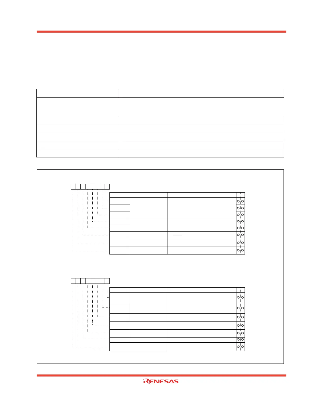
Table 1.35: Repeat-sweep mode 1 specification
Figure 1.103: A-D conversion register in repeat-sweep mode 1
Item Specification
Function
All pins perform repeat sweep A-D conversion, with emphasis on the pin or
pins selected by the A-D sweep pin select bit
Example: AN
0
selected AN
0 ->
AN
1 ->
AN
0 ->
AN
2 ->
AN
0 ->
AN
3
, etc.
Start condition Writing “1” to A-D conversion start flag
Stop condition Writing “0” to A-D conversion start flag
Interrupt request generation timing None generated
Input pin AN
0
(1 pin), AN
0
and AN
1
(2 pins), AN
0
to AN
2
(3 pins), AN
0
to AN
3
(4 pins)
Reading of result of A-D converter Read A-D register corresponding to selected pin (at any time)
A-D control register 0
(Note)
Symbol
Address
When reset
ADCON0
03D6
16
00000XXX
2
b7 b6 b5 b4 b3 b2 b1 b0
Analog input pin
select bit
CH0
Bit symbol Bit name Function
CH1
CH2
A-D operation mode
select bit 0
1 1 : Repeat sweep mode 1
MD0
MD1
Trigger select bit 0 : Software trigger
1 : AD
TRG
trigger
TRG
ADST
A-D conversion start flag 0 : A-D conversion disabled
1 : A-D conversion started
Frequency select bit 0
0 : f
AD
/4 is selected
1 : f
AD
/2 is selected
CKS0
WR
A-D control register 1 (Note)
Symbol
Address
When reset
ADCON1
03D7
16
00
16
Bit name FunctionBit symbol
b7 b6 b5 b4 b3 b2 b1 b0
A-D sweep pin select bit
SCAN0
SCAN1
MD2
BITS
8/10-bit mode select bit
0 : 8-bit mode
1 : 10-bit mode
VCUT
Vref connect bit
1 : Repeat sweep mode 1
A-D operation mode
select bit 1
1 : Vref connected
WR
1
1
Invalid in repeat sweep mode 1
1
Note: If the A-D control register is rewritten during A-D conversion, the conversion result
is indeterminate.
b4 b3
When repeat sweep mode 1 is selected
0 0 : AN
0
(1 pin)
0 1 : AN
0
, AN
1
(2 pins)
1 0 : AN
0
to AN
2
(3 pins)
1 1 : AN
0
to AN
3
(4 pins)
b1 b0
1
Note: If the A-D control register is rewritten during A-D conversion, the conversion result
is indeterminate.
Frequency select bit 1
0 : f
AD
/2 or f
AD
/4 is selected
1 : f
AD
is selected
CKS1
0
0
Reserved bit
Always set to "0
"
 Loading...


