Performance outline
M30240 Group
Rev.1.00 Sep 24, 2003 Page 5 of 360
1.1.5 Performance outline
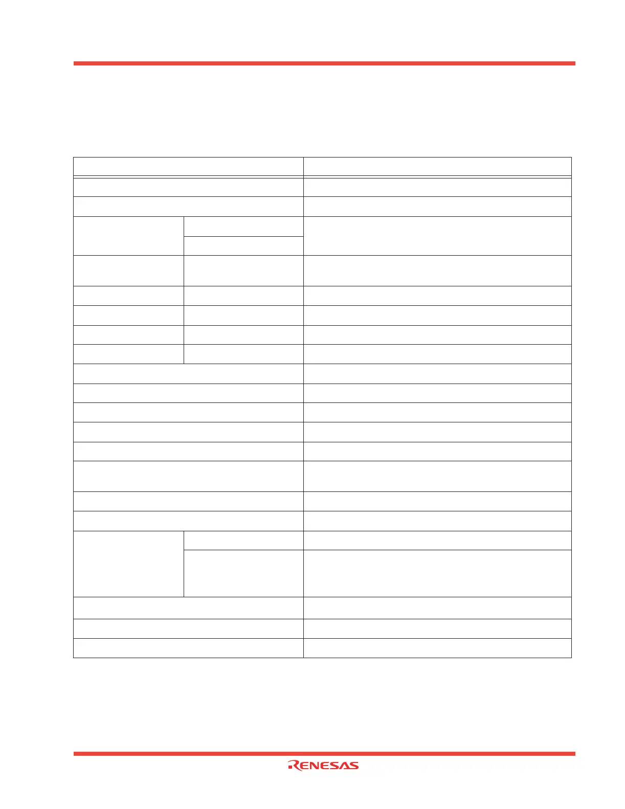
Table 1.1 is a performance outline of the M30240 group.
Table 1.1: Performance outline of M30240 group
Item Performance
Number of basic instructions 91 instructions
Shortest instruction execution time
83ns (f(X
IN) =12MHz)
Memory capacity
ROM
(See Table 1.2: ROM capacity field)
RAM
I/O port
P0 to P3, P6,P7, P8
(except P85), P10
8 bits x 7, 7 bits x 1
Input port P85 1 bit x 1
Multifunction Timer TA0, TA1, TA2, TA3, TA4 16 bits x 5
General purpose Timer TB0, TB1, TB2 16 bits x 3
Serial I/O UART0, UART1, UART2 (UART or clock synchronous) x 3
A-D converter 10 bits x 8 channels
DMAC 2 channels (trigger:19 sources)
CRC calculation circuit CRC-CCITT
Watchdog timer 15 bits x 1 (with prescaler)
Interrupt 21 internal and 4 external sources, 4 software sources, 7 levels
Clock-generating circuit
Built-in clock generation circuit (built-in feedback resistor, and
external ceramic or quartz oscillator)
Supply voltage (typical) 4.1 to 5.25V, (f(X
IN)=12MHz, without software wait)
Power consumption (typical) 250 mW, Vcc=5.0V, 12MHz
I/O characteristics
I/O withstand voltage 5V
Average output current
5 mA available on ports P0, P1, P3,P6, P7
1
, P7
3
, P7
5
, P7
7
,
P8
1
~P8
4
, P8
6
, P8
7
, P10
10 mA available on ports P2, P7
0
, P7
2
, P7
4
, P7
6
, P8
0
Operating temperature
0 to 70
o
C
Device configuration CMOS high performance silicon gate
Package 80-pin plastic molded QFP
 Loading...


