A-D Converter
M30240 Group
Rev.1.00 Sep 24, 2003 Page 241 of 360
2.6.2.5 Repeat-sweep mode 0
In repeat-sweep 0 mode, select functions from those listed in Table 2.31 . An example using the
indicated options is described below. Figure 2.87 shows the timing chart, and Figure 2.88 shows the set-
up procedure.
Table 2.31: A-D converter in repeat-sweep mode 0 functions
Operation
(1) Setting the A-D conversion start flag to “1” causes the A-D converter to start the conversion on the
voltage input to the AN
0
pin.
(2) After the A-D conversion of the voltage input to the AN
0
pin is completed, the content of the suc-
cessive comparison register (conversion result) is transmitted to A-D register 0.
(3) The A-D converter converts all pins selected by the user. The conversion result is transmitted to
A-D register i corresponding to each pin every time A-D conversion on the pin is completed. The A-D
conversion interrupt request bit does not go to “1”.
(4) The A-D converter continues operating until the A-D conversion start flag is set to “0” by software.
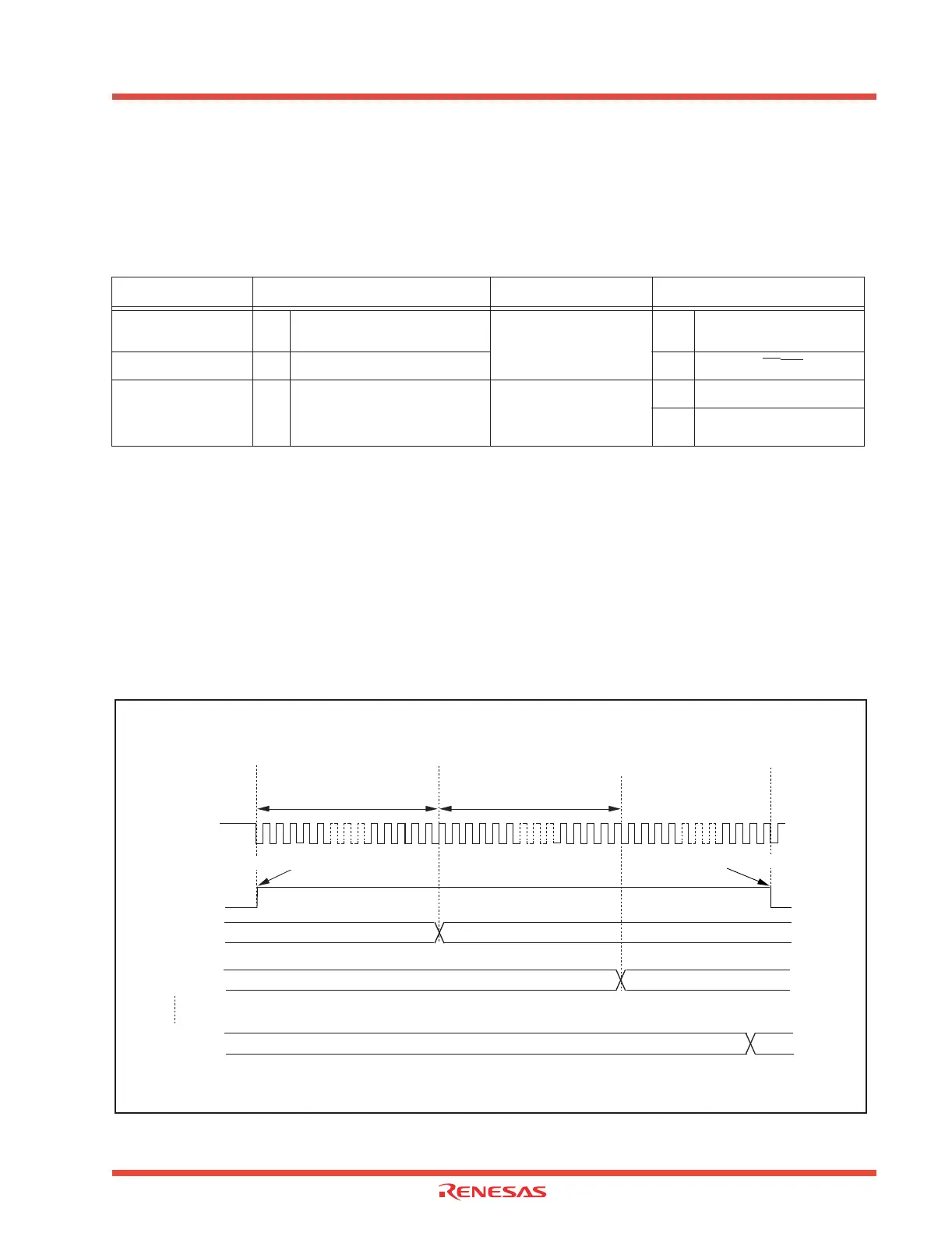
Figure 2.87: Operation timing of repeat sweep mode 0
Item
Set-up Item Set-up
Operation clock AD O
Divided-by-4 fAD/ divided-by-2
fAD/fAD
Trigger for starting A-D
conversion
O Software trigger
Resolution O 8-bit / 10-bit Trigger by AD
TRG
Analog input pin O
AN
0
pin and AN
1
(2 pins) / AN
0
to AN
3
(4 pins) / AN
0
to AN
5
(6
pins) / AN
0
to AN
7
(8 pins)
Sample & Hold
Not activated
O Activated
(2) AN1 conversion begins after AN0
conversion is complete
A-D
conversion
start flag
“1”
“0”
A-D register 0
A-D register 1
φAD
A-D register i
Result
Result
Result
8-bit resolution : 28 φAD cycles
10-bit resolution : 33
φAD cycles
8-bit resolution : 28
φAD cycles
10-bit resolution : 33
φAD cycles
(3) Consecutive conversion
A-D conversion
is complete
(1) Start A-D conversion
Set to “1” by software.
Cleared to “0” by software
(4)
 Loading...


