Frequency Synthesizer
M30240 Group
Rev.1.00 Sep 24, 2003 Page 288 of 360
3.1 Frequency Synthesizer
This section explains how to setup the frequency synthesizer for USB operation.
3.1.1 Outline
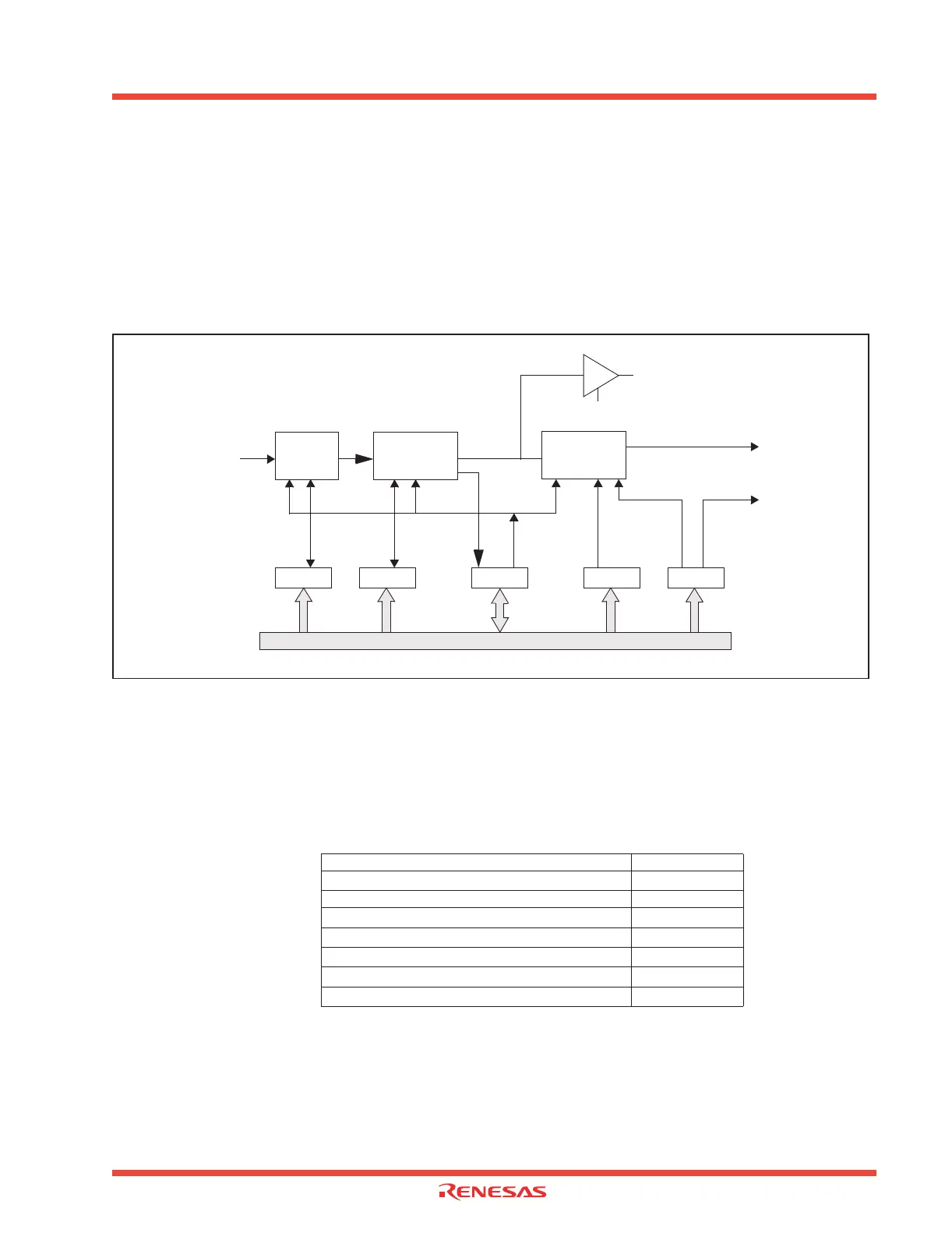
The frequency synthesizer generates the 48MHz clock that is necessary for the USB block and the fSYN
clock. These clocks are a multiple of the external input standard clock f(XIN). Figure 3.1 shows the
frequency synthesizer circuit block diagram.
Figure 3.1: Frequency Synthesizer Circuit Block Diagram
3.1.2 Related Registers
Table 3.1 shows a memory location diagram for the frequency synthesizer related registers; Figures 3.3
and 3.4 show the composition of the frequency synthesizer related registers.
Table 3.1: Frequency Synthesizer-Related Registers Memory Locations
Address Register Name Acronym
000A
16
Protect Register PRCR
03DB
16
Frequency Synthesizer Clock Control Register FSCCR
03DC
16
Frequency Synthesizer Control Register FSC
03DD
16
Frequency Synthesizer Multiply Register FSM
03DE
16
Frequency Synthesizer Pre-Scaler Register FSP
03DF
16
Frequency Synthesizer Division Register FSD
FSP
Data Bus
FSM FSC FSD
03DE
16
03DD
16
03DC
16
03DF
16
Frequency
Multiplier
Frequency
Divider
8 Bit
LS
8 Bit
f(Xin)
f
VCO
f
SYN
f
USB
Prescaler
8 Bit
f
PIN
FSCCR
FSCCR0
03DB
16
EN
USBC5
 Loading...


