Frequency Synthesizer Circuit
M30240 Group
Rev.1.00 Sep 24, 2003 Page 39 of 360
1.2.17.2 Multiplier
Clock f
VCO
is a multiplied up version of clock f
PIN
(See Figure 1.25). The relationship between f
VCO
and the clock input to the multiplier (f
PIN
) from the prescaler is as follows:
• f
VCO
= f
PIN
x 2(n+1) where n is the decimal equivalent of the value loaded in FSM.
Setting FSM to 255 disables the multiplier and f
VCO
= f
PIN
.
Note 1: n must be chosen such that f
VCO
equals 48 MHz.
Note 2: Minimum f
PIN
is 1 MHz.
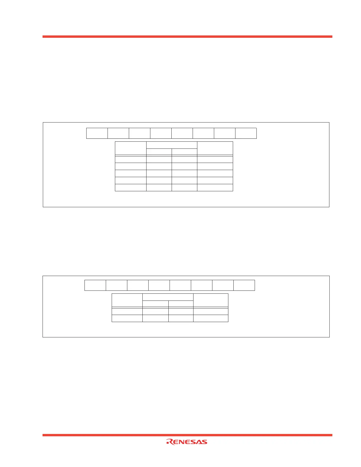
Figure 1.25: Frequency Synthesizer Multiply Register (FSM)
1.2.17.3 Divider
Clock f
SYN
is a divided down version of clock f
VCO
(See Figure 1.26). The relationship between f
SYN
and the clock input to the divider (f
VCO
) from the multiplier is as follows:
• f
SYN
= f
VCO
/ 2(m+1) where m is the decimal equivalent of the value loaded in FSD.
Setting FSD to 255 disables the divider and f
SYN
= f
VCO
.
Figure 1.26: Frequency Synthesizer Divide Register (FSD)
f
PIN
x 2(n+1) = f
VCO
f
PIN
FSM
f
VCO
Dec(n) Hex(n)
1 MHz 23 17 48.00 MHz
2 MHz 11 0B 48.00 MHz
4 MHz 5 05 48.00 MHz
6 MHz 3 03 48.00 MHz
12 MHz 1 01 48.00 MHz
MSB
7
LSB
0
Bit 6 Bit 1 Bit 0
Bit 2
Bit 5Bit 4Bit 3Bit 7
Address: 03DD
16
Access: R/W
Reset: FF
16
f
VCO
/2(m+1) = f
SYN
f
VCO
FSD
f
SYN
Dec(m) Hex(m)
48.00 MHz 1 01 12.00 MHz
48.00 MHz 127 7F 187.50 KHz
MSB
7
LSB
0
Bit 6 Bit 1 Bit 0
Address: 03DF
16
Access: R/W
Reset: FF
16
Bit 2
Bit 5Bit 4Bit 3
Bit 7
 Loading...


