A-D Converter
M30240 Group
Rev.1.00 Sep 24, 2003 Page 252 of 360
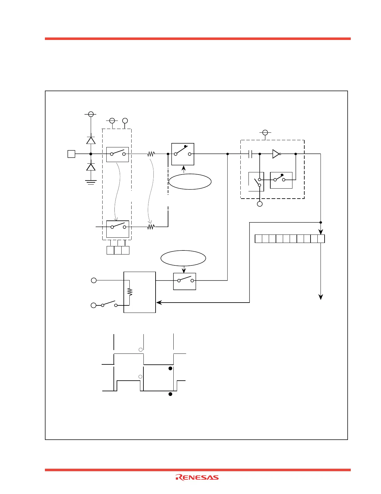
2.6.6 Internal Equivalent Circuit
Figure 2.98 shows the internal equivalent circuit of analog input.
Figure 2.98: Internal equivalent circuit to analog input
ON resistor
approx. 2kΩ
A-D successive conversion
register
Analog input voltage
AVcc
AVss
Chopper-type
amplifier
ADT/A-D conversion
interrupt request
Vcc Vss
V
IN
A-D control register 0
Comparison voltage
Comparison reference voltage (Vref) generator
V
REF
AVss
Vref
b2 b1 b0
Vcc
Vss
AN i
Wiring resistor
approx. 0.2kΩ
ON resistor
approx. 0.6kΩ
SW2
Sampling
control signal
SW1
C = Approx. 3.0pF
SW3
SW4
AMP
ON resistor,
approx. 5kΩ
SW2
Reference control
signal
Resistor
ladder
Control signal
for SW2
Control signal
for SW3
Connect to
Connect to
Comparison
Connect to
Connect to
Sampling
i ladder-type
switches
i ladder-type wiring
resistors
ON resistor
approx. 0.6kΩ
AN0
Parasitic
diode
SW1
SW1 conducts only on the ports selected for analog input.
SW2 and SW3 are open when A-D conversion is not in
progress; their status varies as shown by the waveforms in
the diagrams on the left.
SW4 conducts only when A-D conversion is not in progress.
Parasitic
diode
Warning: Use only as a standard for designing this data.
Mass production may cause some changes in device characteristics.
(i = 10)
(i = 10)
 Loading...


