Block Diagram
M30240 Group
Rev.1.00 Sep 24, 2003 Page 4 of 360
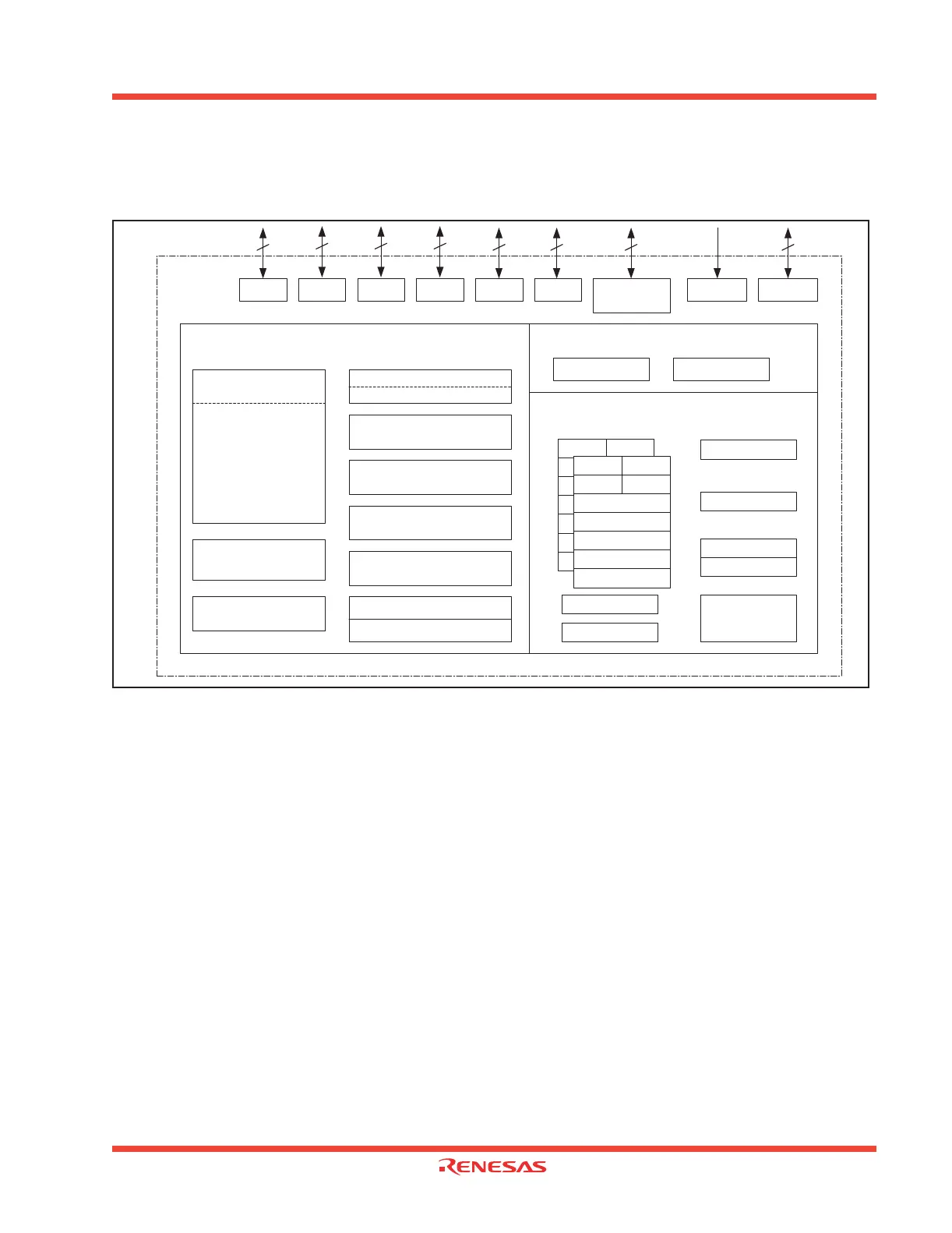
1.1.4 Block Diagram
Figure 1.2 is a block diagram of the M30240 group.
Figure 1.2: Block diagram of M30240 group
Timer
Timer TA0 (16 bits)
Timer TA1 (16 bits)
Timer TA2 (16 bits)
Timer TA3 (16 bits)
Timer TA4 (16 bits)
Timer TB0 (16 bits)
Timer TB1 (16 bits)
Timer TB2 (16 bits)
Watchdog timer
(1 line)
DMAC
(2 channels)
System clock generator
X
IN
- X
OUT
A-D converter
10 bits x 8 channels
USB function control unit
Frequency Synthesizer
UART/clock synchronous S I/O
(8 bits x 3 channels) Note
CRC arithemetic circuit (CCITT)
(Polynomial: X
16
+X
12
+X
5
+1)
Internal peripheral functions
SB
FLG
PC
Registers Program counter
INTB
Vector table
Stack Pointer
ISP
USP
Multiplier
M16C series 16-bit CPU core
Memory
ROM RAM
Port P0 Port P1 Port P2 Port P3 Port P6 Port P7
Port P8
0
~P8
4
,
P8
6
, P8
7
Port P8
5
Port P10
I/O Ports
8
8
8 8
8 8 87
Note: One serial I/O can be used for SIM interface
R0H R0L
R0H R0L
R1H R1L
R2
R3
A0
A1
FB
 Loading...


