Clock-Synchronous Serial I/O
M30240 Group
Rev.1.00 Sep 24, 2003 Page 190 of 360
2.4.2.2 Transfer clock output from multiple pins function selected
In transmitting data in clock-synchronous serial I/O mode, select functions from those listed in Table
2.15 . An example using the indicated options is described below. Figure 2.48 shows the operation
timing, and Figure 2.49 and Figure 2.50 show the set-up procedures.
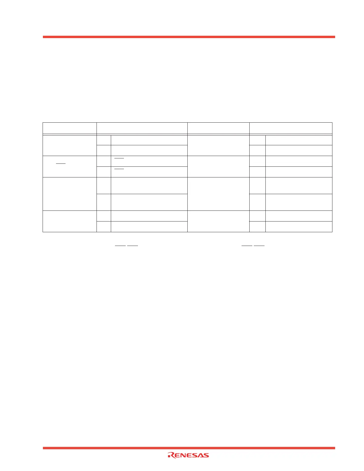
Table 2.15: Serial I/O transmission in clock-synchronous serial I/O mode, transfer clock output from
multiple pins function
Note 1: This can be selected only when UART1 is used in combination with the internal clock. When this function is
selected, the UART1 CTS
/RTS function cannot be utilized. Set the UART1 CTS/RTS disabled bit to “1”.
Note 2: UART2 only.
Operation
(1) Setting the transmit enable bit to “1” makes data transmission status ready.
(2) When transmission data is written to the UART1 transmit buffer register, transmission data held in
the UART1 transmit buffer register is transmitted to the UART1 transmit register in synchronization
with the first falling edge of the transfer clock. At this time, the first bit of the transmission data is trans-
mitted from the TxD1 pin. Then the data is transmitted bit by bit from the lower order in synchronization
with the falling edges of the transfer clock.
(3) When transmission of 1-byte of data is completed, the transmit register empty flag goes to “1”,
which indicates that the transmission is completed. The transfer clock stops at “H” level. At this time,
the UART1 transmit interrupt request bit goes to “1”.
(4) Setting CLK/CLKS select bit 1 to “1” and setting CLK/CLKS select bit 0 to “1” causes the CLKS1
pin to go to the transfer clock output pin. Change the transfer clock output pin when transmission is
halted.
Item
Set-up Item Set-up
Transfer clock source
O Internal clock (f1/f8/f32)
Transmission interrupt
factor
Transmission buffer empty
External clock (CLKi pin) O Transmission complete
CTS
function
CTS
function enabled
Output transfer clock to
multiple pins (Note 1)
Not selected
O CTS
function disabled O Selected
CLK polarity
O
Output transmission data at the
falling edge of the transfer clock
Data logic select function
(Note 2)
O No reverse
Output transmission data at the
rising edge of the transfer clock
Reverse
Transfer clock
O LSB first
TxD, RxD I/O polarity
reverse bit (Note 2)
O No reverse
MSB first Reverse
 Loading...


