Central Processing Unit
M30240 Group
Rev.1.00 Sep 24, 2003 Page 10 of 360
1.2 Operation of Functional Blocks
The M30240 group accommodates certain units in a single chip. These units include ROM and RAM to
store instructions and data, and the central processing unit (CPU) to execute arithmetic/logic operations.
Also included are peripheral units such as USB, timers, serial I/O, DMAC, CRC calculation circuit, A-D
converter, and I/O ports.
The following explains each unit.
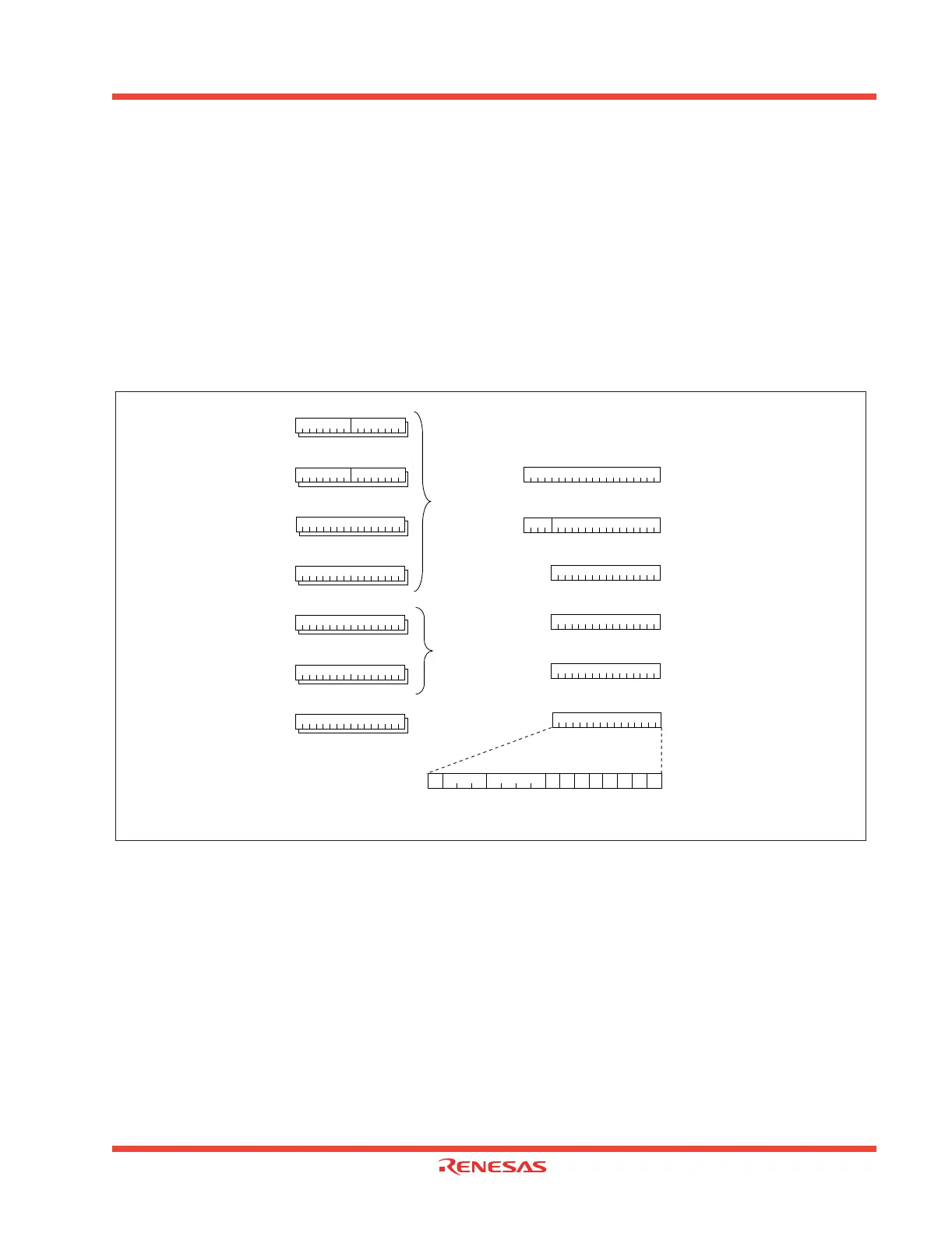
1.2.1 Central Processing Unit
The CPU has a total of 13 registers shown in Figure 1.5. Seven of these registers (R0, R1, R2, R3, A0,
A1, and FB) come in two sets; therefore, these have two register banks.
Figure 1.5: Central processing unit register
1.2.1.1 Data registers
Data registers (R0, R1, R2, and R3) are configured with 16 bits, and are used primarily for transfer
and arithmetic/logic operations.
Registers R0 and R1 each can be used as separate 8-bit data registers, high-order bits as (R0H/R1H),
and low-order bits as (R0L/R1L). In some instructions, registers R2 and R0, as well as R3 and R1, can
be used as 32-bit data registers (R2R0/R3R1).
1.2.1.2 Address registers (A0 and A1)
Address registers (A0 and A1) are configured with 16 bits, and have functions equivalent to those of
data registers. These registers can also be used for address register indirect addressing and address
register relative addressing.
In some instructions, registers A1 and A0 can be combined for use as a 32-bit address register (A1A0).
H
L
b15
b8 b7 b0
R0
(Note)
H
L
b15 b8 b7 b0
R1
(Note)
R2
(Note)
b15 b0
R3
(Note)
b15
b0
A0
(Note)
b15
b0
A1
(Note)
b15 b0
FB
(Note)
b15 b0
Data
registers
Address
registers
Frame base
registers
b15
b0
b15 b0
b15
b0
b15
b0
b0 b19
b0
b19
HL
Program counter
Interrupt table
register
User stack pointer
Interrupt stack
pointer
Static base
register
Flag register
PC
INTB
USP
ISP
SB
FLG
Note:
These registers consist of two register banks.
CDZSBOIU
IPL
 Loading...


