Timer B
M30240 Group
Rev.1.00 Sep 24, 2003 Page 76 of 360
1.2.22 Timer B
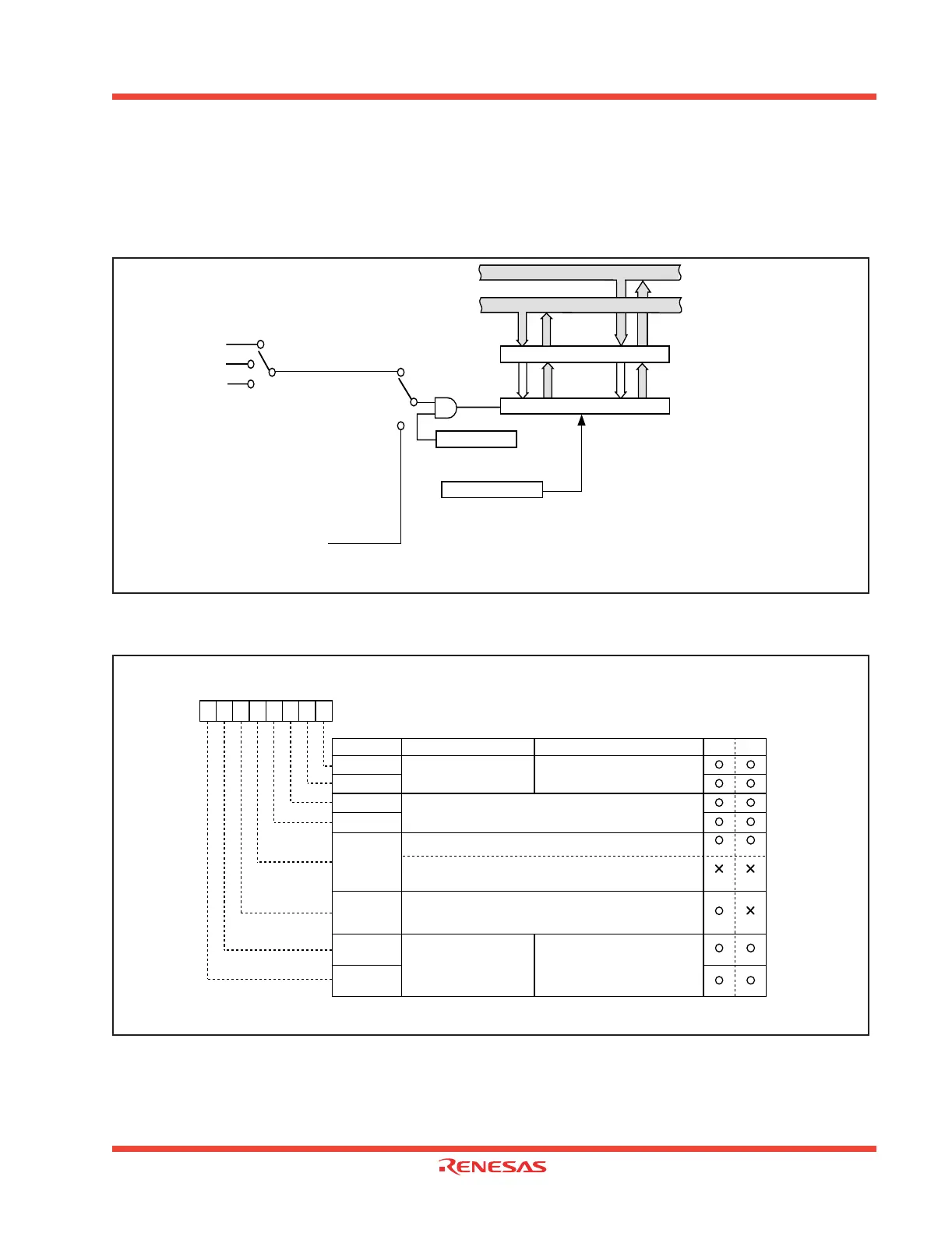
Figure 1.70 shows the block diagram of timer B. Figure 1.71 and Figure 1.72 show the Timer B-related
registers. Use the Timer Bi mode register (i = 0 to 2) bits 0 and 1 to choose the desired mode. Timer B
works in Timer mode only (i.e., the timer counts an in internal count source).
Figure 1.70: Block diagram of Timer B
Figure 1.71: Timer B-related registers (1)
Clock source selection
(address 0380
16
)
Reload register (16)
Low-order 8 bits
Data bus low-order bits
Data bus high-order bits
f1
f8
f32
TBj overflow
j = i – 1.
Note, however,
Count start flag
Counter reset circuit
Counter (16)
TBi Address TBj
Timer B0 0391
16
0390
16
Timer B2
Timer B1 0393 0392 Timer B0
j = 2 when i = 0
Timer B2 0395
16
0394
16
Timer B1
16
16
High-order 8-bits
Note 1: Timer B0.
Note 2: Timer B1, Timer B2.
Timer Bi mode register
Symbol Address
When reset
TBiMR(i=0 to 2) 039B
16 to 039D16
00XX0000
2
Bit name Function
Bit symbol WR
b7 b6 b5 b4 b3 b2 b1 b0
Operation mode select bit
0 0 : Timer mode
b1 b0
TMOD1
TMOD0
MR0
Invalid in timer mode
Can be “0” or “1”
MR2
MR1
MR3
0 0 : f
1
0 1 : f8
1 0 : f32
1 1 : Reserved
TCK1
TCK0
Count source select bit
0
0
0 (Fixed to “0” in timer mode ; i = 0)
(Note 1)
(Note 2)
b7 b6
Nothing is assigned (i=1,2). In an attempt to write to this bit, write "0".
The value, if read, turns out to be indeterminate.
Invalid in timer mode. In an attempt to write to this bit, write "0".
The value, if read, turns out to be indeterminate.
 Loading...


