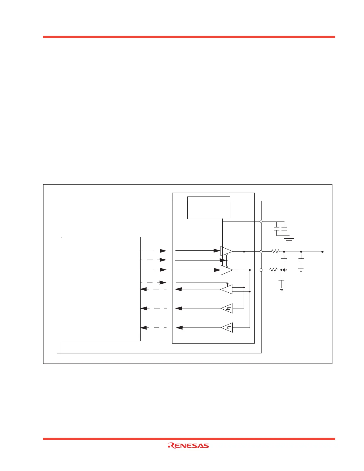
USB Transceiver
M30240 Group
Rev.1.00 Sep 24, 2003 Page 136 of 360
1.5.4 USB Transceiver
When using the on-chip voltage converter to supply the necessary 3.3V to the driver circuit, a capacitor
network must be connected between Ext. Cap (pin 6) and V
SS
(pin 13). Two capacitors are required
as shown in Figure 1.21. The high frequency 0.1
µ
F
capacitor should be
an X7R type or better. The
low frequency decoupling capacitor of 2.2
µ
F
should be of tantalum di-electric or better.
The start-up
time for this value of the capacitor is 3.2
ms, approximately (1ms/
µ
F
) + 1 ms.
After enabling the on-chip voltage converter, a certain amount of time must pass before a wait or stop
clock instruction is executed. The amount of time is given by (C+1)
ms, when C is the value in
µ
F
of
the external capacitance connected to the Ext. Cap pin. For example, if the external capacitance is 2.2
µ
F
, at least 3.2 ms must elapse from the time that the on-chip voltage converter is enabled until a WAIT
instruction or STOP command (CM10 = 1) is executed.
In order to meet the impedance matching requirements of the USB Specification, a 27
Ω-33Ω resistor
must be added to USB D+ (pin 9) and to USB D- (pin 10). In addition, capacitors connected between
USB D+ and USB D- or USB D+/D- and Vss may need to be added for rise/fall time matching and
edge control. These capacitors should be placed after the 33
Ω resistors. Their configuration and val-
ues will depend on the PCs layout. The placement of external components is illustrated in Figure .
Figure 1.121: Configuration of External USB components
27-33
Ω
27-33
Ω
+
_
D+
D-
XCV_Vm_in
XCV_Vp_in
XCV_Rxd
XCV_Vp_out
XCV_Suspend
XCV_Vm_out
XCV_Txen_n
Transceiver
USB_Vp_out
USB_Txen_n
USB_Vm_out
USB_Suspend
USB_Rxd
USB_Vp_in
USB_Vm_in
USB Block
Voltage Converter
2.2
µ
F 0.1
µ
F 10%
EXTCAP
22 pF
22 pF
10%
33 pF
(Note)
Note: Capacitor and resistor values and configuration may depend on PCB layout.
 Loading...


