EasyManua.ls Logo

Renesas M16C Series User Manual

Renesas M16C Series
380 pages
To Next Page IconTo Next Page
To Previous Page IconTo Previous Page
Page #337 background imageLoading...
Page #337 background image
Universal Serial Bus
M30240 Group
Rev.1.00 Sep 24, 2003 Page 319 of 360
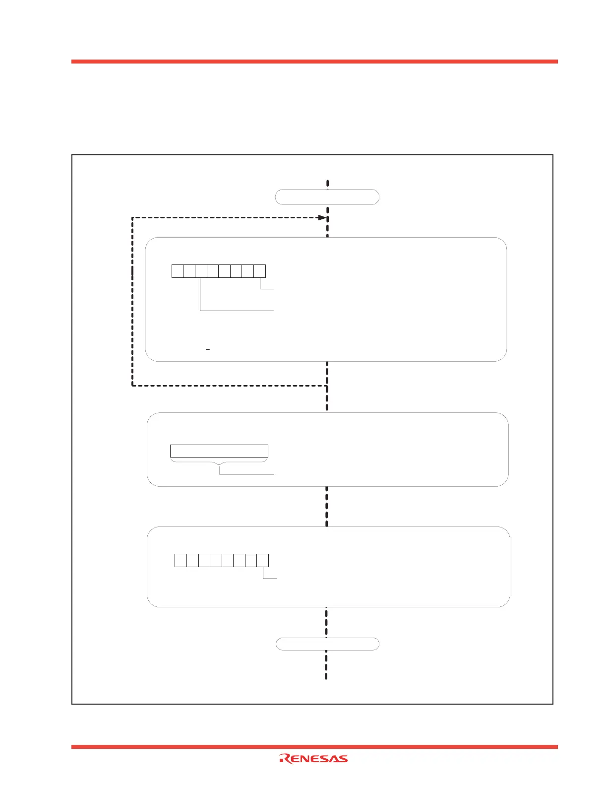
3.2.10 USB Transmission (IN)
Figure 3.32 shows the procedures for Endpoints 1-4 USB IN transmission. Use caution when using
isochronous transfer and the UNDER_RUN is “1” because a USB Endpoint x IN interrupt will occur.
Figure 3.32: Procedures for sending USB Transmission
USB Endpoint x FIFO Address
EPi (i = 1-4) 0339
16, 033A16,
033B16, 033C16
Transmission Data
b7
b0
Setting Transmission Data IN FIFO
USB Endpoint x IN Interrupt Processing Routine
Confirm Data Transmission in FIFO
USB Endpoint x IN Control and Status Register Address
EPiICS (i = 1-4) 0319
16, 032116,
032916, 033116
IN_PKT_RDY Bit
0 : Not ready
1 : Ready
TX_NOT_EPT Bit (Note)
o : Transmit FIFO is empty
1 : Transmit FIFO is not empty
b7 b0
Register Evacuation Process
Note: In the case of double buffer mode, 1 data packet remains in FIFO when the IN_PKT_RDY is "0" and the TX_NOT_EPT
is "1" (packet size < half FIFO size.) When the remaining data is transmitted with the next IN token, the TX_NOT_EPT is
automatically cleared.
Setting IN_PKT_RDY
USB Endpoint x IN Control and Status Register Address
EPiICS (i = 1-4) 0319
16, 032116,
032916, 033116
IN_PKT_RDY Bit (Note)
1 : Data Packet Ready
b7 b0
Note: If the transmission data is a short packet or if the AUTO-SET bit is "0" the user must set to "1".
1
Register Recover Processing
Execute REIT Command
0
0

Table of Contents

Question and Answer IconNeed help?

Do you have a question about the Renesas M16C Series and is the answer not in the manual?

Renesas M16C Series Specifications

General IconGeneral
Architecture16-bit
CoreM16C
Instruction Set ArchitectureCISC
Flash MemoryUp to 512 KB
Operating Voltage2.7V to 5.5V
Operating Temperature Range-40°C to +85°C
Package TypesLQFP, QFP
TimersMultiple 16-bit timers
ADC10-bit
Communication InterfacesUART, SPI, I2C
InterruptsMultiple interrupt sources

Summary

Chapter 1: Hardware

1.1 Description

Overview of the M30240 group as a single-chip USB peripheral microcontroller based on M16C family.

1.1.1 Features

Lists the key features of the M30240 group, including CPU, USB capabilities, memory, voltage, and peripherals.

1.1.3 Pin Configuration

Shows the pin configuration (top view) of the M30240 group, detailing each pin's name, I/O, and basic function.

1.1.4 Block Diagram

Presents a block diagram illustrating the internal structure and major components of the M30240 group.

1.1.5 Performance outline

Details the performance specifications of the M30240 group, including instruction count, memory capacity, and I/O ports.

1.1.6 Pin Description

Provides a detailed description of each pin of the M30240 microcontroller, including its name, I/O type, and functions.

CHAPTER 2: PERIPHERAL FUNCTIONS USAGE

2.1 Protect

Explains the protect function to prevent unintended changes to important registers when a program runs away.

2.2 Timer A

Provides an overview and detailed operation modes of the 16-bit Timer A, including timer, event counter, and PWM modes.

2.3 Timer B

Details the operation and registers of Timer B, a 16-bit timer that operates only in timer mode.

2.4 Clock-Synchronous Serial I/O

Explains clock-synchronous serial communication, including transmission/reception formats, transfer rates, and error detection.

2.5 Clock-Asynchronous Serial I/O (UART)

Covers UART operations, including transmission/reception formats, transfer rates, error detection, and functions like SIM interface compliance.

2.6 A-D Converter

Describes the A-D converter, its modes of operation, conversion clock, conversion time, and related registers.

2.7 DMAC

Explains the DMAC (Direct Memory Access Controller) for data transfer between memory and peripherals without CPU intervention.

2.10 Address Match Interrupt

Explains the address match interrupt functionality for simplified debugging, including enable/disable and timing.

2.11 Key-Input Interrupt

Describes the key-input interrupt, which is generated by falling edges on Port 0 or Port 1 pins used as input.

2.12 Power Control

Explains power control modes (Normal, Wait, Stop) for reducing CPU power consumption by stopping oscillators or clocks.

2.13 Programmable I/O Ports

Details the programmable I/O ports, including direction registers, port registers, pull-up control, and high drive capacity.

Chapter 3 Universal Serial Bus

3.1 Frequency Synthesizer

Explains how to set up and use the frequency synthesizer to generate the 48MHz clock for USB and DC-DC converter power.

3.2 Universal Serial Bus

Provides an overview of the Universal Serial Bus (USB) features, including specification compatibility, error handling, and transfer types.

3.2.2 USB Related Registers

Lists and describes USB-related registers for controlling USB functionality, including control, status, and enable registers.

3.2.7 USB Interrupts

Details the types of USB interrupts (Function, Reset, Resume, SOF, Suspend) and their handling via enable flags and priority levels.

3.2.8 USB Function Control Unit Initialization

Outlines the initialization routine for the USB Function Control Unit, including frequency synthesizer setup and endpoint initialization.

3.2.9 USB Control Transfers and SET_ADDRESS Request

Explains USB control transfers, the SET_ADDRESS request, and procedures for setting the device address.

Chapter 4 Interrupts

4.1 Overview of Interrupts

Provides an overview of interrupt types, including software, hardware, special, and peripheral I/O interrupts.

4.1.1 Type of Interrupts

Classifies interrupts into maskable and non-maskable types, detailing software and hardware interrupt categories.

4.1.2 Interrupt Vector Tables

Describes interrupt vector tables, including fixed and variable types, and lists interrupts assigned to fixed vector tables.

4.1.3 Interrupt Control

Explains interrupt control registers, interrupt request bits, enable flags, and priority levels for managing interrupts.

4.1.4 Interrupt Sequence

Details the sequence of operations when an interrupt occurs, including saving registers and processor control flow.

4.1.5 Multiple Interrupts

Explains how multiple interrupts are handled, including priority levels and interrupt acceptance conditions.

Chapter 5 Built-in PROM Version

5.1 Built-in PROM Version

Introduces the built-in PROM version, its functions, and available types (OTP and EPROM).

5.1.1 Outline

Outlines the capabilities of the built-in PROM version, including programming methods and suitability for different production volumes.

5.2 EPROM version

Describes the EPROM version, its operating modes (Normal, EPROM), and related pins.

5.2.1 EPROM mode pins

Lists pin functions specifically for the EPROM mode, detailing their roles in programming and verification.

5.2.2 Input/Output signals

Explains the input/output signals for Read, Program, and Erase operations in EPROM mode.

5.2.3 Algorithm Programming

Details the step-by-step algorithm for programming the built-in PROM, including voltage settings and pulse application.

5.3 Usage Precaution

Provides precautions for using built-in PROM versions, including handling of high voltage and protection of the EPROM window.

5.3.1 Built-in PROM versions

Offers specific cautions for programming built-in PROM versions, emphasizing voltage and power-on sequences.

5.3.2 One-time PROM versions

Highlights that OTP versions are not tested/screened, recommending programming and testing for reliability.

5.3.3 EPROM versions

Advises on protecting the EPROM window from light and cleaning it before erasure for optimal performance.

Chapter 6 Standard Characteristics

6.1 Standard DC Characteristics

Presents standard DC characteristics of the M30240EC, including output currents and voltage ratings.

Related product manuals