Programmable I/O Ports
M30240 Group
Rev.1.00 Sep 24, 2003 Page 115 of 360
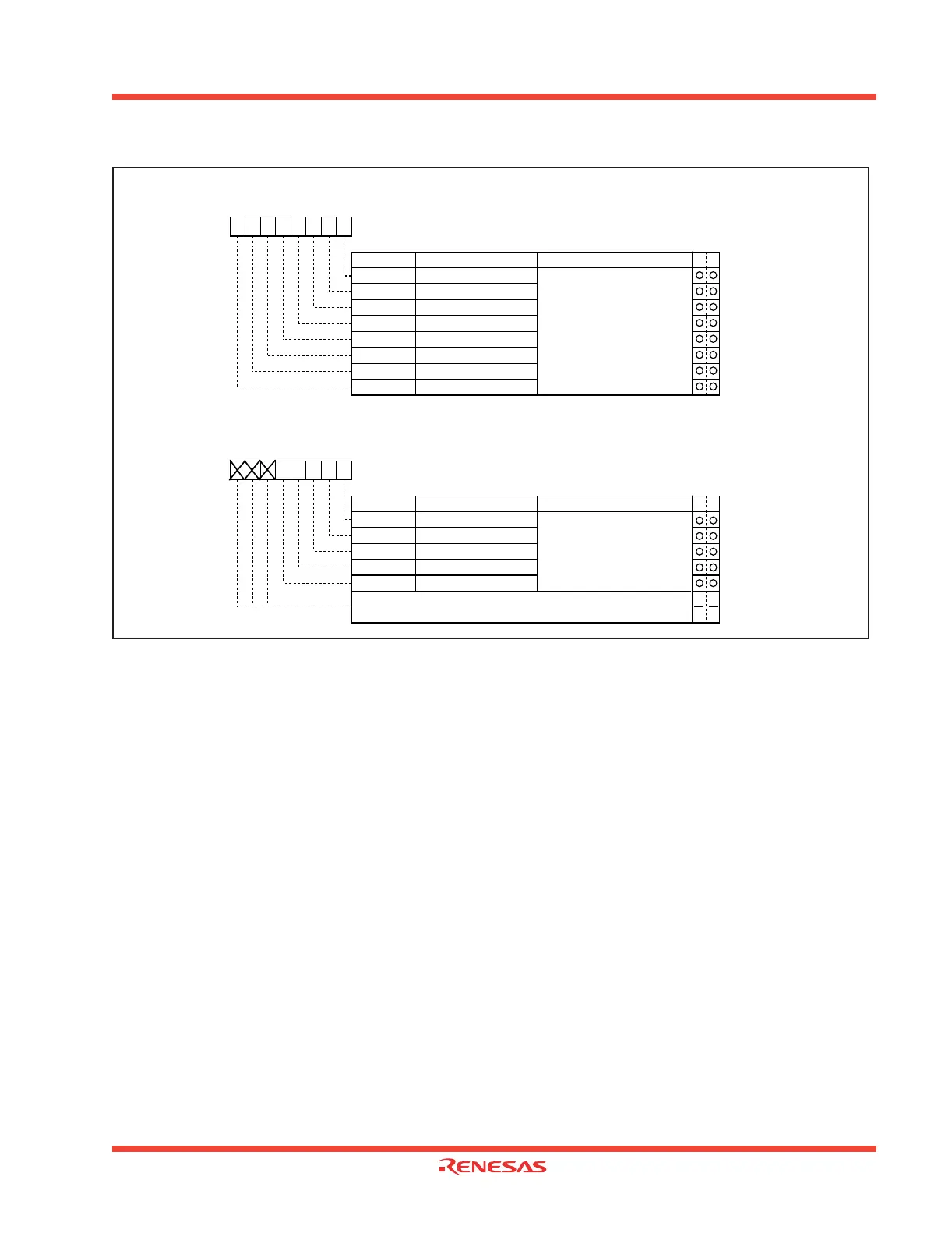
Figure 1.112: Port 2 and Timer A Output drive capacity registers
Port 2 Drive Capacity register
Symbol
Address When reset
P2DR
03FA 16 0016
Bit name Function Bit symbol WR
b7 b6 b5 b4 b3 b2 b1 b0
P2DR0 P2
0
LED drive capacity
P2DR1 P2
1
LED drive capacity
P2DR2 P2
2
LED drive capacity
P2DR3 P2
3
LED drive capacity
P2DR4 P2
4
LED drive capacity
P2DR5 P2
5
LED drive capacity
P2DR6 P2
6
LED drive capacity
P2DR7 P2
7
LED drive capacity
The N-channel high-drive capacity
is activated for the corresponding
bit.
0 : Normal drive
1 : N-channel high drive
Timer A Output Drive
Capacity register
Symbol
Address When reset
TADR
03FB16 0016
Bit name Function Bit symbol WR
b7 b6 b5 b4 b3 b2 b1 b0
TADR0 TA0 OUT drive capacity
TADR1 TA1
OUT drive capacity
TADR2 TA2
OUT drive capacity
TADR3 TA3
OUT drive capacity
TADR4 TA4
OUT drive capacity
High-drive capacity is activated for
the corresponding TAi
OUT pin.
0 : Normal drive
1 : High drive
Nothing is assigned. These bits can neither be
set nor reset.
When read, their contents are "0".
 Loading...


