Clock-Synchronous Serial I/O
M30240 Group
Rev.1.00 Sep 24, 2003 Page 195 of 360
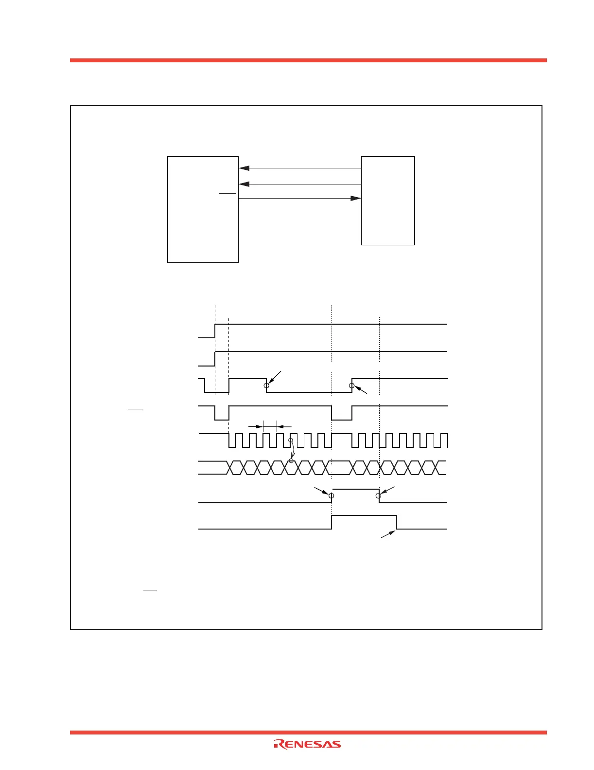
Figure 2.51: Operation timing of reception in clock-synchronous serial I/O mode
CLKi
R
X
Di
RTSi
CLK
T
X
D
Port
Microcomputer
Transmitter side IC
Example of wiring
Example of operation
1 / fEXT
Transmit enable
bit (TE)
Transmit buffer
empty flag (Tl)
CLKi
RxDi
Receive complete
flag (Rl)
RTSi
“H”
“L”
“0”
“1”
“0”
“1”
“0”
“1”
Receive enable
bit (RE)
“0”
“1”
The above timing applies to the following settings:
• External clock is selected.
• RTS function is selected.
• CLK polarity select bit = “0”.
fEXT: frequency of external clock
Make sure that the following conditions are met when
the CLKi pin input =“H” before data reception
• Transmit enable bit → “1”
• Receive enable bit → “1”
• Dummy data written to UARTi transmit buffer register
Receive interrupt
request bit (IR)
“0”
“1”
Cleared to “0” when interrupt request is accepted, or cleared by software
D
0
D1 D2
D3
D4 D5
D6
D7
D0
D1 D2
D3
D4 D5
Shown in ( ) are bit symbols.
Reception data is taken in
Transferred from UARTi receive register
to UARTi receive buffer register
(1) Reception enabled
(2) Start reception
(3) Reception is complete
Read out from UARTi receive buffer register
Transferred from UARTi transmit buffer register to UARTi transmit register
(4) Read of reception data
Dummy data is set in UARTi transmit buffer register
 Loading...


