EasyManua.ls Logo

Renesas M16C Series User Manual

Renesas M16C Series
380 pages
To Next Page IconTo Next Page
To Previous Page IconTo Previous Page
Page #223 background imageLoading...
Page #223 background image
Clock-Asynchronous Serial I/O
M30240 Group
Rev.1.00 Sep 24, 2003 Page 205 of 360
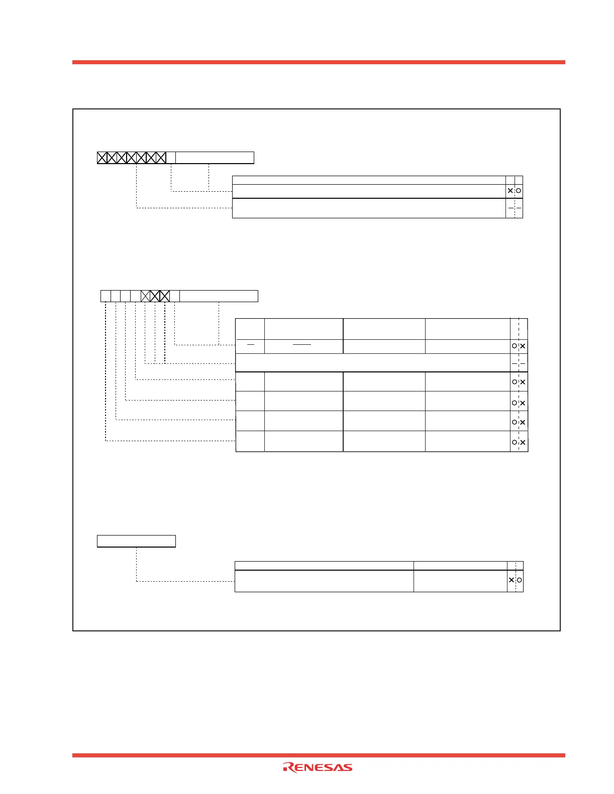
Figure 2.57: UARTi related registers (1)
b7
UARTi bit rate generator
b0
Symbol
Address
When reset
U0BRG
03A1
16
Indeterminate
U1BRG
03A9
16
Indeterminate
U2BRG
0379
16
Indeterminate
Function
Assuming that set value = n, BRGi divides the count source by
n + 1
0016 to FF16
Values that can be set
WR
b7 b0
(b15) (b8)
b7 b0
UARTi transmit buffer register
Function
Transmit data
Nothing is assigned.
In an attempt to write to these bits, write “0”. The value, if read, turn out to be indeterminate.
Symbol
Address
When reset
U0TB
03A3
16, 03A216
Indeterminate
U1TB
03AB
16, 03AA16
Indeterminate
U2TB
037B
16, 037A16
Indeterminate
WR
(b15)
Symbol Address When reset
U0RB 03A7
16, 03A616 Indeterminate
U1RB 03AF
16, 03AE16 Indeterminate
U2RB 037F
16, 037E16 Indeterminate
b7 b0
(b8)
b7 b0
UARTi receive buffer register
Function
(During UART mode)
Function
(During clock synchronous
serial I/O mode)
Bit name
Bit
symbol
0 : No framing error
1 : Framing error found
0 : No parity error
1 : Parity error found
0 : No error
1 : Error found
Note : Bits 15 through 12 are set to “0” when the serial I/O mode select bit (bits 2 to 0 at addresses 03A0
16,
03A8
16 and 037816) are set to “0002” or the receive enable bit is set to “0”.
(Bit 15 is set to “0” when bits 14 to 12 all are set to “0”.) Bits 14 and 13 are also set to “0” when the
lower byte of the UARTi receive buffer register (addresses 03A6
16 , 03AE16 and 037E16) is read out.
Invalid
Invalid
Invalid
OER
FER
PER
SUM
Overrun error flag (Note)
Framing error flag
Parity error flag
Error sum flag
0 : No overrun error
1 : Overrun error found
0 : No overrun error
1 : Overrun error found
Nothing is assigned.
These bits cannot be set or reset. When read, the value of these bits is “0”.
WR
Receive data
Receive data
(Note)
(Note)
(Note)

Table of Contents

Question and Answer IconNeed help?

Do you have a question about the Renesas M16C Series and is the answer not in the manual?

Renesas M16C Series Specifications

General IconGeneral
Architecture16-bit
CoreM16C
Instruction Set ArchitectureCISC
Flash MemoryUp to 512 KB
Operating Voltage2.7V to 5.5V
Operating Temperature Range-40°C to +85°C
Package TypesLQFP, QFP
TimersMultiple 16-bit timers
ADC10-bit
Communication InterfacesUART, SPI, I2C
InterruptsMultiple interrupt sources

Summary

Chapter 1: Hardware

1.1 Description

Overview of the M30240 group as a single-chip USB peripheral microcontroller based on M16C family.

1.1.1 Features

Lists the key features of the M30240 group, including CPU, USB capabilities, memory, voltage, and peripherals.

1.1.3 Pin Configuration

Shows the pin configuration (top view) of the M30240 group, detailing each pin's name, I/O, and basic function.

1.1.4 Block Diagram

Presents a block diagram illustrating the internal structure and major components of the M30240 group.

1.1.5 Performance outline

Details the performance specifications of the M30240 group, including instruction count, memory capacity, and I/O ports.

1.1.6 Pin Description

Provides a detailed description of each pin of the M30240 microcontroller, including its name, I/O type, and functions.

CHAPTER 2: PERIPHERAL FUNCTIONS USAGE

2.1 Protect

Explains the protect function to prevent unintended changes to important registers when a program runs away.

2.2 Timer A

Provides an overview and detailed operation modes of the 16-bit Timer A, including timer, event counter, and PWM modes.

2.3 Timer B

Details the operation and registers of Timer B, a 16-bit timer that operates only in timer mode.

2.4 Clock-Synchronous Serial I/O

Explains clock-synchronous serial communication, including transmission/reception formats, transfer rates, and error detection.

2.5 Clock-Asynchronous Serial I/O (UART)

Covers UART operations, including transmission/reception formats, transfer rates, error detection, and functions like SIM interface compliance.

2.6 A-D Converter

Describes the A-D converter, its modes of operation, conversion clock, conversion time, and related registers.

2.7 DMAC

Explains the DMAC (Direct Memory Access Controller) for data transfer between memory and peripherals without CPU intervention.

2.10 Address Match Interrupt

Explains the address match interrupt functionality for simplified debugging, including enable/disable and timing.

2.11 Key-Input Interrupt

Describes the key-input interrupt, which is generated by falling edges on Port 0 or Port 1 pins used as input.

2.12 Power Control

Explains power control modes (Normal, Wait, Stop) for reducing CPU power consumption by stopping oscillators or clocks.

2.13 Programmable I/O Ports

Details the programmable I/O ports, including direction registers, port registers, pull-up control, and high drive capacity.

Chapter 3 Universal Serial Bus

3.1 Frequency Synthesizer

Explains how to set up and use the frequency synthesizer to generate the 48MHz clock for USB and DC-DC converter power.

3.2 Universal Serial Bus

Provides an overview of the Universal Serial Bus (USB) features, including specification compatibility, error handling, and transfer types.

3.2.2 USB Related Registers

Lists and describes USB-related registers for controlling USB functionality, including control, status, and enable registers.

3.2.7 USB Interrupts

Details the types of USB interrupts (Function, Reset, Resume, SOF, Suspend) and their handling via enable flags and priority levels.

3.2.8 USB Function Control Unit Initialization

Outlines the initialization routine for the USB Function Control Unit, including frequency synthesizer setup and endpoint initialization.

3.2.9 USB Control Transfers and SET_ADDRESS Request

Explains USB control transfers, the SET_ADDRESS request, and procedures for setting the device address.

Chapter 4 Interrupts

4.1 Overview of Interrupts

Provides an overview of interrupt types, including software, hardware, special, and peripheral I/O interrupts.

4.1.1 Type of Interrupts

Classifies interrupts into maskable and non-maskable types, detailing software and hardware interrupt categories.

4.1.2 Interrupt Vector Tables

Describes interrupt vector tables, including fixed and variable types, and lists interrupts assigned to fixed vector tables.

4.1.3 Interrupt Control

Explains interrupt control registers, interrupt request bits, enable flags, and priority levels for managing interrupts.

4.1.4 Interrupt Sequence

Details the sequence of operations when an interrupt occurs, including saving registers and processor control flow.

4.1.5 Multiple Interrupts

Explains how multiple interrupts are handled, including priority levels and interrupt acceptance conditions.

Chapter 5 Built-in PROM Version

5.1 Built-in PROM Version

Introduces the built-in PROM version, its functions, and available types (OTP and EPROM).

5.1.1 Outline

Outlines the capabilities of the built-in PROM version, including programming methods and suitability for different production volumes.

5.2 EPROM version

Describes the EPROM version, its operating modes (Normal, EPROM), and related pins.

5.2.1 EPROM mode pins

Lists pin functions specifically for the EPROM mode, detailing their roles in programming and verification.

5.2.2 Input/Output signals

Explains the input/output signals for Read, Program, and Erase operations in EPROM mode.

5.2.3 Algorithm Programming

Details the step-by-step algorithm for programming the built-in PROM, including voltage settings and pulse application.

5.3 Usage Precaution

Provides precautions for using built-in PROM versions, including handling of high voltage and protection of the EPROM window.

5.3.1 Built-in PROM versions

Offers specific cautions for programming built-in PROM versions, emphasizing voltage and power-on sequences.

5.3.2 One-time PROM versions

Highlights that OTP versions are not tested/screened, recommending programming and testing for reliability.

5.3.3 EPROM versions

Advises on protecting the EPROM window from light and cleaning it before erasure for optimal performance.

Chapter 6 Standard Characteristics

6.1 Standard DC Characteristics

Presents standard DC characteristics of the M30240EC, including output currents and voltage ratings.

Related product manuals