A-D Converter
M30240 Group
Rev.1.00 Sep 24, 2003 Page 247 of 360
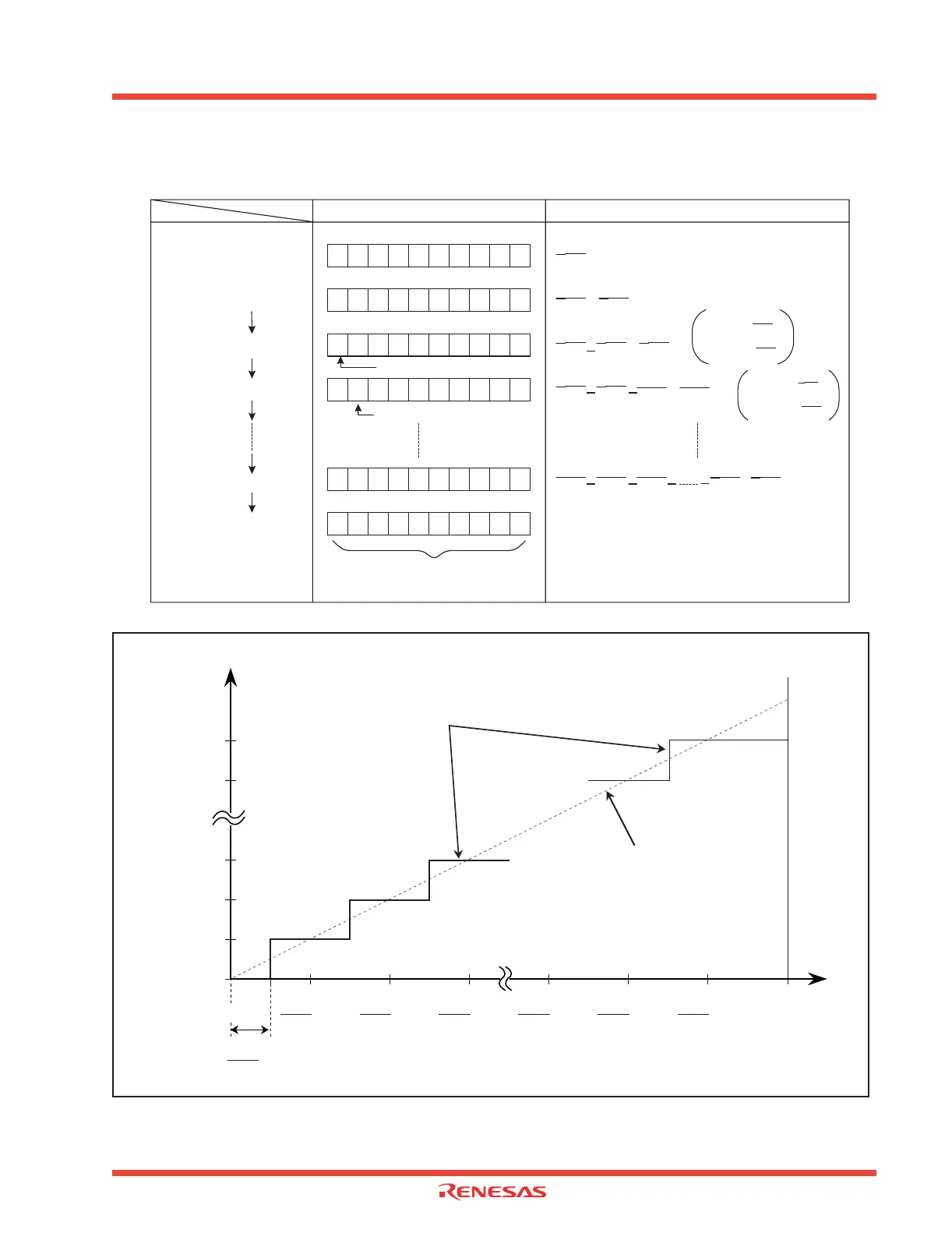
Table 2.34: Variation of successive comparison register and VREF while A-D conversion is in progress
(10-bit mode)
Figure 2.93: Theoretical A-D conversion characteristics (10-bit mode)
b9 b0
1 0 0 0 0 0 0 0 0 0
1 0 0 0 0 0 0 0 0 0
n9
1 0 0 0 0 0 0 0 0
n9 n8
1 0 0 0 0 0 0 0
n9 n8 n7 n6 n5 n4 n3 n2 n1 1
n9 n8 n7 n6 n5 n4 n3 n2 n1 n0
VREF
2
VREF
2
VREF
2
VREF
2
VREF
2
[V]
VREF
2048
[V]
VREF
2048
VREF
4
[V]
VREF
4
VREF
8
VREF
2048
VREF
4
VREF
8
VREF
1024
VREF
2048
[V]
[V]
n9=1 + VREF
4
n9=0 - V
REF
4
n8=1 + VREF
8
n8=0 - V
REF
8
A-D converter stopped
1st comparison
2nd comparison
3rd comparison
10th comparison
Conversion complete
1st comparison result
2nd comparison result
This data transfers to bit 0 and
bit 9 of A-D register
+
+ +
+ + +
+
-
-
-
-
Successive approximation register VREF change
00016
00116
00216
00316
3FE16
3FF16
Result of A-D conversion
Analog input voltage
VREF
1024
x 1
VREF
1024
x 2
VREF
1024
x 3
x 1021
V
REF
1024
VREF
1024
x 1022
VREF
1024
x 1023
VREF
VREF
1024
x 0.5
Theoretical A-D
conversion characteristic
Ideal A-D conversion
characteristic
0
 Loading...


