3.1 Mounting and Connections
455
7SD5 Manual
C53000-G1176-C169-1
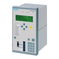
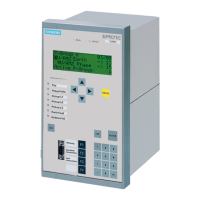
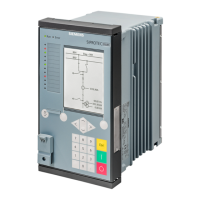
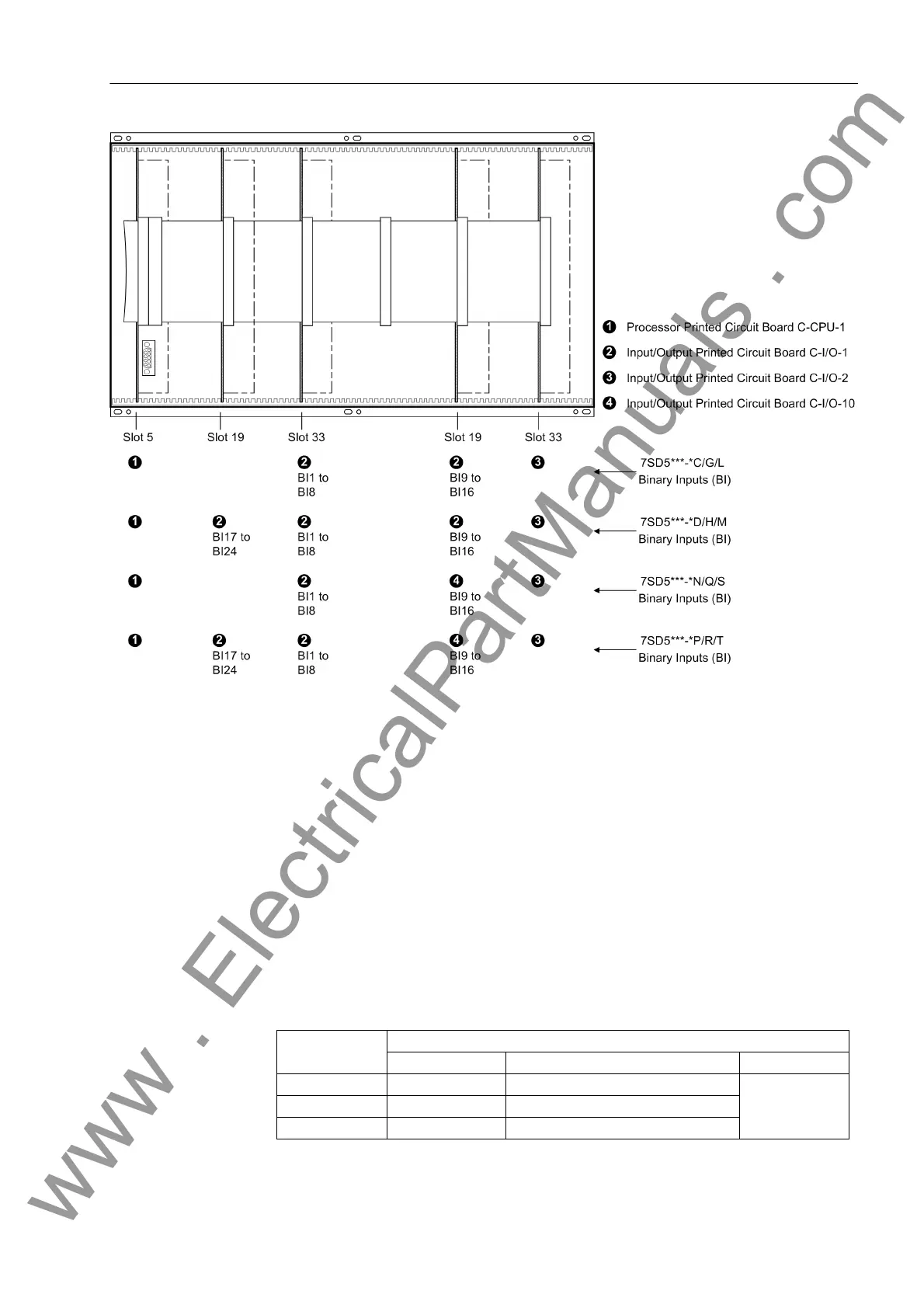
Figure 3-4 Front view with housing size
1
/
1
after removal of the front cover (simplified and scaled down)
3.1.2.3 Switching Elements on Printed Circuit Boards
Input/Output Board
C-I/O-1 and C-I/O- 10
The layout of the PCB for the input/output board C-I/O-1 is shown in Figure 3-5, the
PCB for the input/output board C-I/O-10 is shown in Figure 3-6.
The power supply is situated
• On the input/output board C-I/O-1 (No. 2 in Figure 3-3, slot 19) for housing size
1
/
2
,
• On the input/output board C-I/O-1 (No. 2 in Figure 3-4, slot 33 left) for housing size
1
/
1
,
The preset nominal voltage of the integrated power supply is checked according to
Table 3-2, the quiescent state of the life contact is checked according to Table 3-3.
Table 3-2 Jumper setting for the nominal voltage of the integrated Power Supply on the
input/output board C-I/O-1
Jumper
Nominal Voltage
60/110/125 VDC 110/125/220/250 VDC 115 VAC 24/48 VDC
X51 1-2 2-3 Jumpers X51 to
X53 are not used
X52 1-2 and 3-4 2-3
X53 1-2 2-3
www . ElectricalPartManuals . com
 Loading...