391
CHAPTER 4 DEVICES
4
4.7 File Register (R)
4.7.1 Storage location
(2) Clearing the file register
If the Latch (2) is set in the Device tab of the PLC parameter dialog box, the data in the file register are not cleared
even if the CPU module is powered off or reset. (Data cannot be initialized by performing latch clear operation.
*1
)
For how to clear the data, refer to the "Data Clear Processing" section. ( Page 75, Section 2.7 (4))
*1 The latch range of the file register can be set in the Device tab of the PLC parameter dialog box. ( Page 395,
Section 4.7.4 (1) (c))
4.7.1 Storage location
File register data are stored in the following memory.
4.7.2 File register size
The size of file register is the total number of points of the file register (ZR), extended data register (D), and extended
link register (W). Set the size so that the total number of points will be less than the free space of memory specified as
a storage location. The free space can be checked in the Confirm Memory Size window using a programming tool.
[Tool] [Confirm Memory Size]
(1) Storing data in the standard RAM
The following table lists the points available for the file register data to be stored in the standard RAM.
Note that if data other than the file register data are stored in the standard RAM, the points will decrease.
( Page 36, Section 2.1.1 (2))
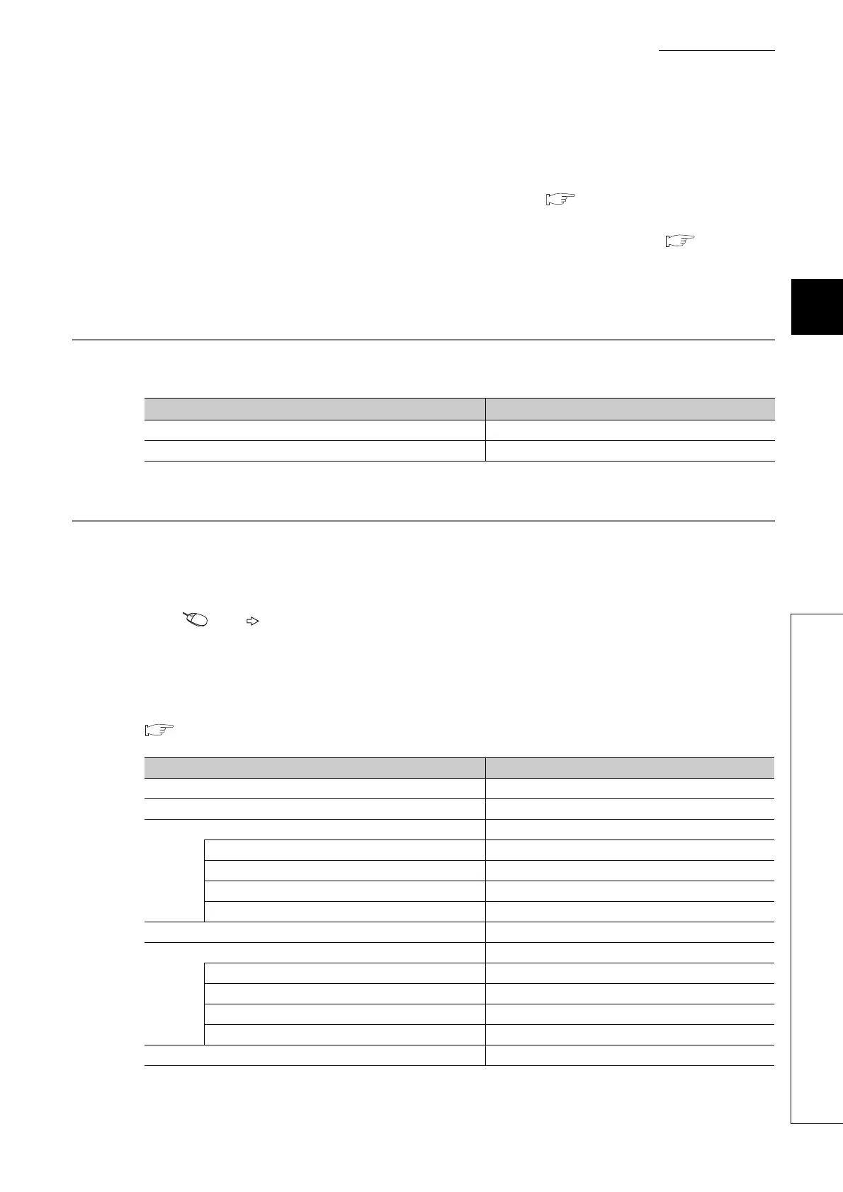
CPU module Memory
Q00UCPU, Q01UCPU, QnUDVCPU, QnUDPVCPU Standard RAM
Q02UCPU, QnUD(H)CPU, QnUDE(H)CPU Standard RAM, SRAM card, Flash card
CPU module Point
Q00UCPU, Q01UCPU, Q02UCPU 64K
Q03UD(E)CPU 96K
Q03UDVCPU 96K
With an extended SRAM cassette (1M) 608K
With an extended SRAM cassette (2M) 1120K
With an extended SRAM cassette (4M) 2144K
With an extended SRAM cassette (8M) 4192K
Q04UD(E)HCPU 128K
Q04UDVCPU, Q04UDPVCPU 128K
With an extended SRAM cassette (1M) 640K
With an extended SRAM cassette (2M) 1152K
With an extended SRAM cassette (4M) 2176K
With an extended SRAM cassette (8M) 4224K
Q06UD(E)HCPU 384K
 Loading...